Apollo Control Computer Architecture
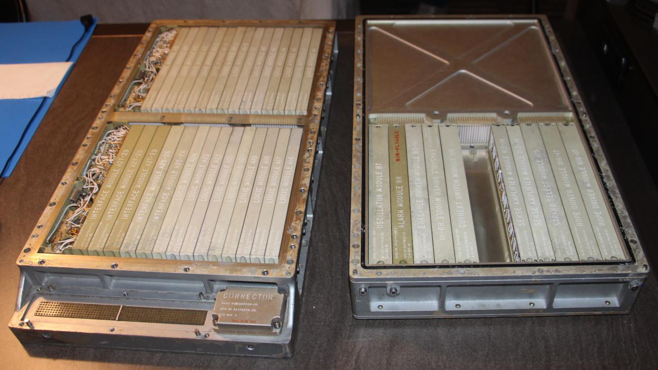
Separated trays of the Apollo control computer. The left tray contains logic based on NOR gates. In the right - memory and auxiliary components.
The Apollo Guidance Computer (AGC) was developed in the 1960s to allow Apollo missions to fly to the moon. At a time when most computers took up space from a full-size refrigerator to an entire room, the AGC was something unique - it was small enough to fit on board the Apollo spacecraft, weighed 32 kg and took no more than 0.03 m 3 (30 liters).
The AGC computer is 15-bit. It is strange to meet a word size that is not a power of two, but in the 1960s, before bytes became popular, computers used a variety of word sizes. 15 bits provided sufficient accuracy for landing on the moon (and used data with double and triple accuracy if necessary), so 16 bits would simply increase the size and weight of the computer unnecessarily.
The AGC instruction was contained in a 15-bit word, and consisted of 3 bits, indicating the operation code, and 12 bits, indicating the address in memory. Unfortunately, these volumes were still not enough, so the computer used numerous tricks and workarounds, and the architecture turned out to be rather awkward. A 12-bit memory address could only access 4K words. At the same time, AGC had 2K words in the main RAM and 36K words in the core memory. To access all memory, AGC used a sophisticated memory bank switching system and multiple registers. In other words, it was possible to access memory only in pieces of 256 words, and ROM - in pieces of a slightly larger size.
3 bits for the operation code was not enough to directly indicate 34 possible instructions, therefore, AGC used tricks with the extension of the value of instructions and with the fact that some instructions made sense to execute only with certain memory cells. In addition, tricks such as “magic” addresses in memory were used - for example, writing to the “shift right register” cell performed a bitwise shift, thus eliminating the need for a separate “right shift” instruction. There were also instructions combining several actions at once.
AGC architecture was pretty simple, even by 1960s standards. Although created in the era of complex and powerful mainframes, AGC's capabilities were very limited; in terms of power and architecture, it is comparable to early microprocessors. Its strengths were its compact size and great capabilities for providing real-time data input and output.
The architectural diagram below shows the main components of the AGC. I highlighted in color the parts that I dwell on in more detail. AGC had a small set of registers, and a simple arithmetic module dealing only with addition. He had only 36K words ROM and 2K words RAM. The “write bus" was the main way of transferring data between components. The decoding instructions and the sequence generator generated control pulses for the AGC.

AGC block diagram
About half of the diagram is occupied by memory, which reflects the fact that in many aspects the AGC architecture was developed around its memory. Like most computers in the 1960s, AGC used core memory by storing each bit in a tiny ferrite ring (core) strung on a wire mesh. Since each bit required a separate physical core, the amount of such memory was radically less than that of a modern semiconductor. A distinctive feature of memory on the cores was that reading a word from memory deleted it, so after each access this value had to be rewritten. AGC also had a fixed ROM memory, the famous stitched cores - they were used to store programs, and were physically stitched with wires (see below).
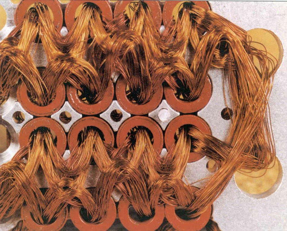
Close-up memory on stitched cores
NOR valves
AGC was one of the first computers to use IP. The possibilities of these first IPs were very limited; on AGC chips (below) there were only six transistors and eight resistors, and together they implemented a NOR gate with three inputs.

Dual NOR valve with three inputs from AGC. Ten wires outside the crystal are connected to the external contacts of the IC.
The schematic designation of the NOR valve is shown below. This is the simplest logic gate: if all inputs are equal to zero, then the output is equal to one. You may be surprised, but one NOR-gate is enough to create a computer. NOR is a universal valve: it can be used to make any other logic valve. For example, when combining all the NOR inputs, we get an inverter. Having placed the inverter at the output of the NOR, we get an OR-valve. By placing the inverters at the inputs of the NOR gate, we get an AND gate. And from these gates, you can build more complex logic: triggers, adders and counters.
The NAND valve has the same versatility. In modern circuits, for technical reasons, NANDs are used more often than NORs. The popular course “ From NAND to Tetris ” describes how to create a computer from NAND valves, right up to the implementation of the Tetris game. First, a set of logic gates is constructed from NAND (NOT, AND, OR, XOR, multiplexer, demultiplexer). Then, larger building blocks (trigger, adder, counter, ALU, register) are created from them, and from them - a computer.

The NOR gate gives 1, if it has 0 on all inputs. If at least one of the inputs has 1, then the NOR gives 0.
Very often in AGC comes across a component such as RS-trigger (set-reset, set / reset). This circuit is made of two NOR gates and stores one data bit. Bit 1 is stored at set input, and bit 0 is stored at reset input. That is, pulse 1, applied to set input, turns off the upper valve and turns on the lower one, so output 1 turns out. Pulse 1, fed to reset input, does the opposite . If 0 is applied to both inputs, the trigger remembers its previous state, playing the role of a drive. In the next section, we will show how registers are made from a trigger.

RS trigger of two NOR gates. One valve, when turned on, turns off the other. A line above one of the outputs indicates that it complements the other.
Registers
AGC has a small set of registers for temporary storage of values outside the main memory. The main register is the drive (A) used in many arithmetic operations. It also has a counter register Z, arithmetic block registers X and Y, buffer B, return address Q, and some others (modern computers use the stack to call subroutines and return from them, but in that era programmers needed to write the stack themselves to recursion ) For access to memory, there is a memory address register S, and for data, a memory buffer register G. Also, AGC has registers in the main memory - for example, input / output counters.
The diagram below shows the AGC register scheme, simplified for the case with one bit and two registers. Each register bit has a trigger using the previously described scheme (blue and purple). Data is transferred to and from the registers via the write bus (red). To write to the register, the trigger is reset by a clear signal (CQG or CZG, green). Then the “write” signal (WQG or WZG, orange) allows the data going along the write bus to set the corresponding register trigger. To read the register, the read signal (RQG or RZG, cyan) passes the trigger output through the recording amplifier to the write bus, and is used in other parts of the AGC. The full register scheme is more complex, it has several 16-bit registers, but the basic scheme is this.

Simplified AGC register operation
The register chart illustrates three key points. Firstly, the register circuit is built from NOR gates. Secondly, data movement is built around the write bus. Finally, the actions of the registers depend on certain control signals arriving at the right time.
Arithmetic module
Most computers have an arithmetic-logic device that performs arithmetic and Boolean operations. Compared to modern computers, the arithmetic module of AGC is very limited: it performs only addition of 16-bit quantities, therefore it is called an arithmetic module and not arithmetic-logical (the rest of the operations are performed through various tricks; for example, subtraction is performed through addition, before which in one of the arguments, the bits are reversed, etc.).
The diagram below shows one bit of the AGC arithmetic module. The full adder (red) calculates the sum of two bits and carry. The transfer is transferred to the next adder - this way they can be combined to add longer words (to speed up the transfer of transfers in cases like 111111111111111 + 1, AGC uses an adder with a transfer skip ).
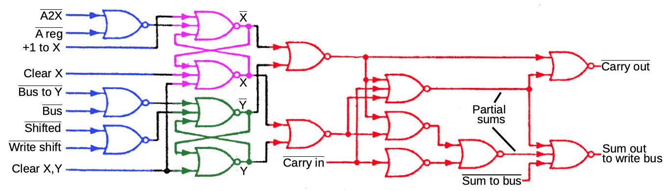
Registers X and Y (purple and green) provide two input bits to the adder. They are implemented using the triggers already described on NOR valves. The blue loop writes the values to the X and Y registers in accordance with the control signals. The scheme is quite complicated, because it allows you to store constants and values with a shift in registers, but I will not go into this topic. Pay attention to the control signal A2X, which transfers the value of register A to register X; we will come back to him later.
The photo below shows the physical implementation of the AGC circuit. This module implements four bits for registers and an arithmetic module. Black rectangles are flat IPs; in each module there are two boards with 60 chips each, and a total of 240 NOR gates. The arithmetic module and registers are assembled from four identical modules, each of which processes four bits; this is similar to the microprocessor section .
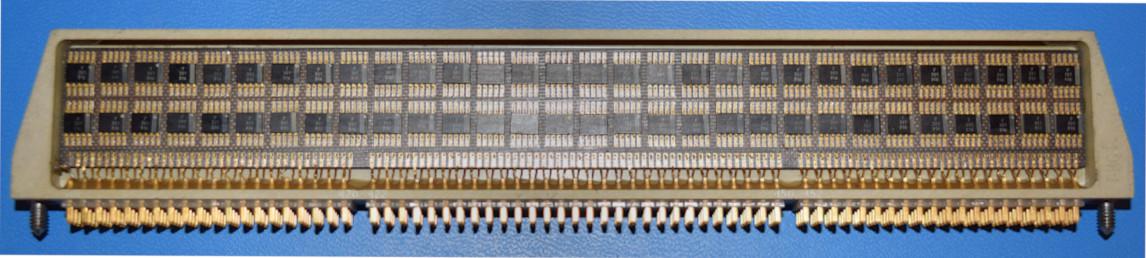
The arithmetic module and registers are assembled from four identical modules. Modules are installed in slots from A8 to A11.
Instruction execution
This section describes the sequence of operations that the AGC performs to execute the instruction. In particular, I will show how the ADS (add to storage) instruction works. This instruction reads the value from memory, adds it to the drive (register A), and saves the sum in both the adder and the memory. This is a single instruction, but for its execution AGC takes several steps and many values are moved here and there.
The instruction timer is implemented due to the memory subsystem on magnetic cores. In particular, reading a value from memory erases the stored value, so after each reading, the value must be written back. Also, when accessing the memory, there is a delay between the designation of the address and the receipt of data. As a result, each clock cycle spends 12 steps for reading and subsequent recording. Each time interval (from T1 to T12) lasts a little less than microseconds, and the entire cycle lasts 11.7 μs, and is called the memory cycle time (MCT).

Erasable magnetic core memory module from AGC. It stores 2 kilosheets, each bit is stored using a separate tiny ferrite ring.
MCT is the basic unit of memory for executing instructions. A typical instruction requires two cycles of memory: one to extract the instruction from memory, the second to perform the operation. Therefore, a typical instruction takes two MCTs (23.4 μs), which gives us 43,000 instructions per second (compared to modern processors and their billions of instructions per second, this is extremely slow).
AGC processes instructions, breaking them into subcommands, each of which takes one clock cycle of memory. For example, an ADS instruction consists of two subcommands: ADS0 (addition) and STD2 (calling the next instruction). The diagram below shows the movement of data within the AGC to execute the ADS0 instruction. 12 measures go from left to right.

The most important steps are as follows:
T1: The operand address is copied from instruction register B to memory address register S to start reading from memory.
T4: The operand is read from memory to memory register G.
T5: The operand is copied from G to adder Y. The value of drive A is copied to adder X.
T6: The adder calculates the sum U, and copies it to the data register of memory G.
T8: The program counter Z is copied to the memory address register S in preparation for receiving the next instruction from memory.
T10: The sum from the data register of memory G is written back to the memory.
T11: Amount U is copied to drive A.
Although this is a simple summing instruction, a lot of data is transferred to and fro over 12 time slots. And with each of these actions a specific control signal is associated; for example, the signal A2X in the interval T5 copies the value from drive A to register X. To copy register G to register Y, two control pulses are required: RG (read G) and WY (write Y). In the next section, I will explain how the AGC control module generates the necessary control signals for each instruction.
Control module
Like most computers, the AGC control module decodes each instruction and generates control signals that tell the rest of the processor what it needs to do. The AGC uses a pre-programmed control module consisting of NOR valves to generate signals. AGC does not use microcode; he has no microinstructions and control memory, as this would take up too much physical space.
The heart of the AGC control module is called the crosspoint generator. It takes a subcommand and one of the time periods and generates control signals for this combination. It can be imagined in the form of a lattice, on which subcommands go in one direction and time segments in the other, and each control point is assigned its own control signal.

The intersection generator requires many components and is divided into three modules; This is the A6 module. Pay attention to the added wires that change the circuit. This is an early version of a module for testing on the ground; flight modules already had no wires.
For efficiency, the final control module is highly optimized. Instructions with similar behavior are combined and processed together by the intersection generator, which reduces the size of the required circuit. For example, AGC has an instruction “add to the drive with double precision” (DAS). Since it is roughly equivalent to two additions of single words, the DAS1 and ADS0 subcommands in the intersection generator have common logic. The diagram below shows the intersection generator circuit for the time interval T5, and the logic of the ADS0 subcommand (using signal DAS1) is highlighted. For example, a 5K signal is generated from a combination of DAS1 and T5.

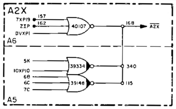
But what are 5K and 5L signals? This is another optimization. Many control pulses are often fed together, so instead of generating them directly, the intersection generator generates intermediate signals for intersections. For example, 5K generates control pulses A2X and RG, and 5L generates control pulse WY. The diagram below shows how the A2X signal is generated: any of 8 different signals (including 5K) generates A2X. Similar circuits generate other control signals. These optimizations made it possible to reduce the size of the intersection generator, but it still remained large, and grew into as many as three modules.
Summing up, we can say that the control module is responsible for telling the CPU what to do to execute the instruction. First, instructions are broken down into subcommands. The intersection generator generates the necessary control pulses for each time interval and subcommand, telling the registers, arithmetic module and memory what they need to do.
Typically, instructions consisted of two subcommands, but there were exceptions. Some of the instructions, such as multiplication or division, required the use of many subcommands, as they consisted of many steps. Conversely, the jump instruction at TC used one subcommand because it only needed to call the next instruction.
Other processors used different approaches to the generation of control signals. 6502 and many other early microprocessors decoded instructions using a programmable logic array (PLA) that implements AND / OR logic through read-only memory.

Microprocessor 6502.
Conclusion
It was an exciting tour of the Apollo on-board control computer. In order not to stretch it much, I concentrated on the ADS addition instructions and some control pulses (A2X, RG and WY). I hope you got an idea of how to assemble a computer from such primitive elements as NOR valves.
The most visible part of the architecture is the data path: an arithmetic module, registers and a data bus. AGC registers are based on simple triggers from NOR gates. And although the AGC arithmetic module can only do addition, the computer can still handle the whole set of operations, including multiplication, division, and Boolean operations.
However, the data path is only part of the computer. Among other critical components, there is a control module that tells the components what they need to do. The approach used in AGC is based on the intersection generator, using highly optimized and hard-coded logic to generate the correct control pulses for specific subcommands and time intervals.
Using these capabilities, the AGC provided guidance, navigation, and control aboard Apollo missions, and made it possible to land on the moon. He also spurred the early integrated circuit industry using 60% of US-made ICs in 1963. Therefore, modern computers owe much to AGC and its simple NOR components.
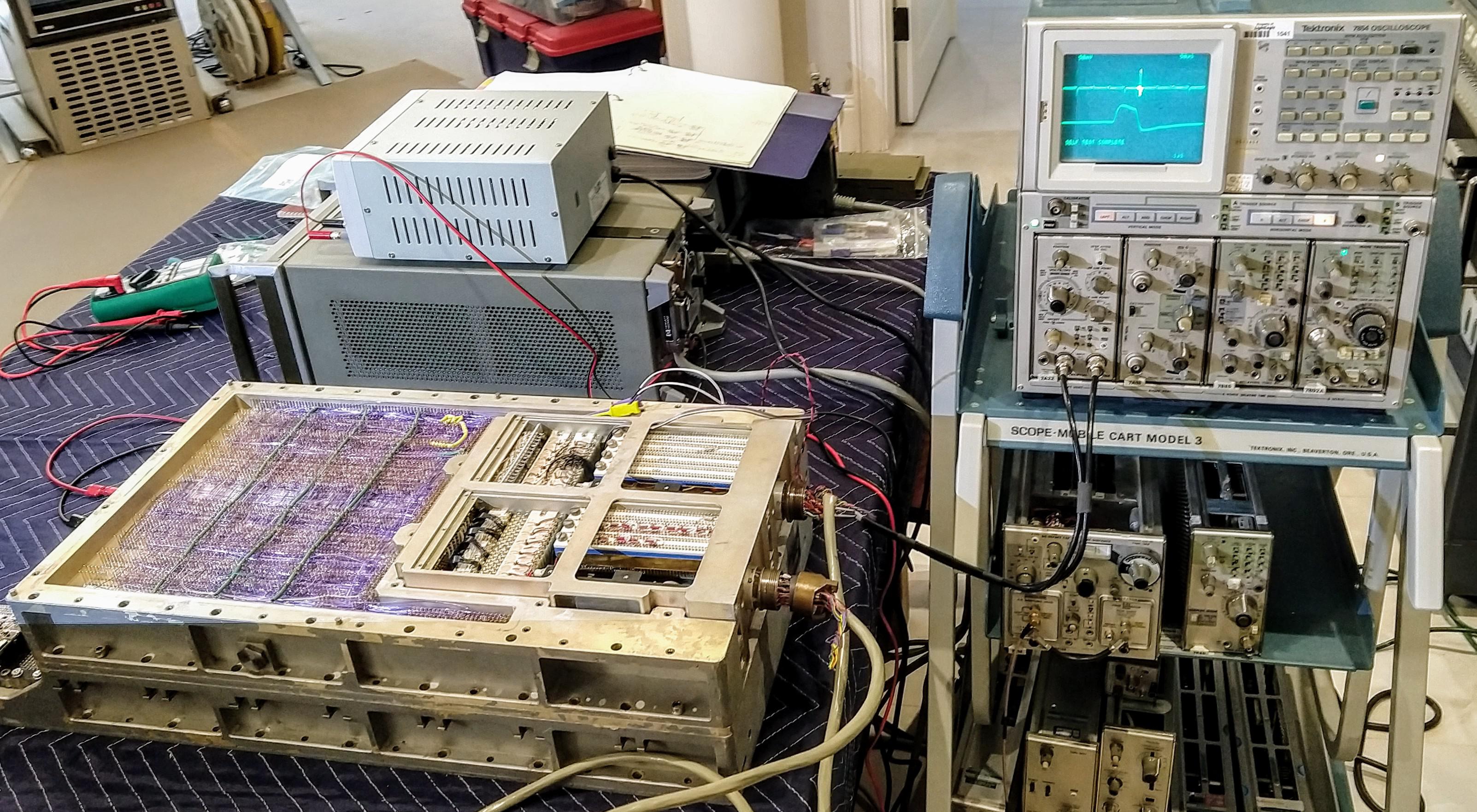
AGC works in a lab connected to a Tektronix vintage oscilloscope