TSMC hopes to be able to follow Moore's law for many more decades
If you thought that Intel’s “gang” is the most faithful adherents of Moore’s law , then you probably haven’t heard how Philip Wong is spreading on this subject. Wong, vice president of corporate research at Taiwan Semiconductor Manufacturing Corp (TSMC), made a presentation at a recent Hot Chips conference stating that Moore’s law is not only alive and well, but with a fairly diverse set of technological tricks, it’s still not true less than three decades.
“He's not dead,” he told those present at Hot Chips. “He doesn't slow down, he doesn't even cough.”
Listen to Wong, so the only necessary action to maintain Moore’s law is to improve density. And although he admits that the clock frequency has hit its ceiling, marking the end of Dennard’s scaling law , he says that it is the density of transistors that will improve speed and energy efficiency.
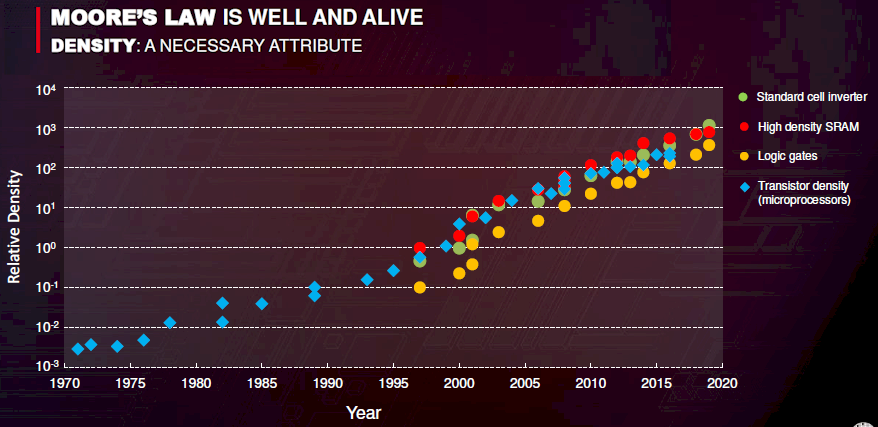
Moore's Law is Alive
Ultimately, it doesn’t matter how much higher density is achieved. Wong believes that the main thing is that companies can stuff more transistors into a smaller volume with better energy efficiency. In the short term, this can be achieved in an old, proven way, namely, by improving the manufacturing technology of CMOS so that it turns out to produce transistors with a shorter gate length.
TSMC has already mastered the 7 nm process technology and is moving towards 5 nm. Wong said that the 5 nm process technology development ecosystem is already ready, and the company has already begun production of risk samples - that is, the process technology and development tools are ready, and work substrates are being produced. At the last meeting of shareholders, TSMC announced that it plans to begin mass production of chips at 5 nm in the first half of 2020. It turns out that the company’s plans already include a 3 nm process technology.
But all this technology is based on planar [flat] chips, and Wong admits that this approach will eventually cease to scale. “If we follow the path of two-dimensional increase, then we have already reached several hundred atoms, and soon all of our atoms will run out,” he explained.
But this does not mean the end of the increase in density. He noted that some innovations in the semiconductor industry supported an upward density chart even at the end of Dennard's scaling. In particular, the technology of strained silicon and high-k dielectric appeared , followed by FInFet (Fin Field Effector Transistor), a technology of three-dimensional structures. Now, to go beyond 7 nm, DTCO (Design Technology Co-Optimization) technology is being investigated.
All these innovations occurred because it was necessary to develop new computing platforms that required faster and more energy-efficient iron. This evolution spawned minicomputers in the 1970s, PCs in the 1980s, the Internet in the 1990s, and today, mobile devices. Each stage required an increase in density through improved semiconductor manufacturing. Wong believes that the following requests will come from artificial intelligence and 5G.
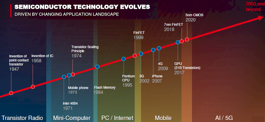
Semiconductor Technology Evolution
What innovations will be required to ensure that Moore's Law party does not stop?
In the short term, the overall computing density and memory density will increase the use of chipsets used to create multi-chip cases of 2.5D structures, even if the chips themselves do not become denser. Wong said that this process is already making the specific process technology of an individual chipset a less important parameter than the ability to integrate these components in a single package.
TSMC has its own version of the 2.5D case with Chip-on-Wafer-on-Substrate (CoWoS) technology (Embedded Multi-die Interconnect Bridge, or EMIB, from Intel competes with this technology). CoWoS allows you to create multi-chip enclosures, securing chipsets and a suitable memory on the interposer, and connect them using the TSV vertical contacts. The most interesting implementation of CoWoS is Nvidia's Tesla V100 GPU Accelerator, in which the GV100 GPU is packed with high bandwidth memory (HBM). More chipsets are being integrated by Intel, AMD and Xilinx.
But the possibilities of 2.5D to increase the density are not unlimited. A more scalable solution will require truly three-dimensional transistor placement technologies. For this, according to Wong, the monolithic three-dimensional technology N3XT is best suited on the basis of new materials and tight integration of memory with logic. N3XT, the "nanoengineering technology of computing systems", has been discussed in academia since 2015, but now that companies such as TSMC have begun to take it seriously, it has a good chance of commercialization.
Wong showed slides with diagrams of how such a device might look. It consists of layers of energy-efficient logic (yellow), high-speed memory (red) and non-volatile memory of high capacity (green), arranged alternately one above the other. And all this sits on an ordinary silicon logic crystal (purple).
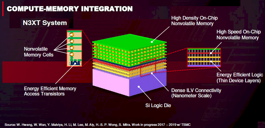
N3XT System
The main thing here is to combine the various layers through ILV, Inter-Layer-Via (interlayer vertical access). Unlike a micrometer scale TSV, ILV can be formed on a nanometer scale. Although this is an extremely important part of the N3XT technology, Wong could tell little about it. It is obvious, however, that TSMC is working closely on it and has already registered several patents related to it.
In three-dimensional chips, the interleaving of memory and logic is very important, since it allows you to reduce the distance between them, thereby ensuring high throughput and low latency of information transfer, which will be necessary for applications such as AI and 5G. In CMOS, memory and logic cannot be interleaved, since etching of logic transistors requires a temperature of the order of 1000 degrees Celsius, which would destroy neighboring layers in production. It requires something that can be manufactured at temperatures of the order of 400 degrees.
It turns out that in the last few years, researchers have studied new materials that seem to be suitable for the production of high-speed transistors at relatively low temperatures. Unlike silicon materials used in production today, monolayers of dichalcogenide transition metals (TMD) are used there on the basis of elements such as molybdenum, tungsten and selenium.
TMD materials demonstrate high mobility of charge carriers - electrons travel through them with great ease - with narrow channels. What is convenient, it is precisely these characteristics that are needed to create transistors with a size of less than 2-3 nm. Wong said the TSMC lab is testing experimental tungsten disulfide-based TMD substrates.
Another candidate for nanomaterials is carbon nanotubes. Wong said their experimental variations were made, showing good material behavior as a semiconductor. Working prototypes of logic and SRAM based on carbon nanotubes have already been assembled, including the RISC-V variant from MIT researchers.
With regard to memory, according to Wong, the most likely candidates for three-dimensional integration will be: SST-MRAM (spin-transfer torque magnetoresistive random access memory, magnetoresistive random access memory, which uses electron spin momentum transfer to record); PCM phase change memory ; random access resistive memory ReRAM; memory based on programmable metallization of CBRAM cell; FERAM ferroelectric random access memory . All this is non-volatile memory with random access, which does not require the operation of erasing a cell before writing new information to it. Some options are already on the market - Everspin MRAM, Samsung MRAM, Crossbar ReRAM and Intel 3D XPoint (which, according to most, is a variant of PCM).

New types of memory
Researchers simulated the performance of N3XT devices and compared them to traditional two-dimensional chips with approximately the same logic and memory capacities. According to their research, where various methods of measuring the speed of machine learning algorithms were used, devices of the N3XT technology turned out to be 63-1971 times more efficient than two-dimensional ones.
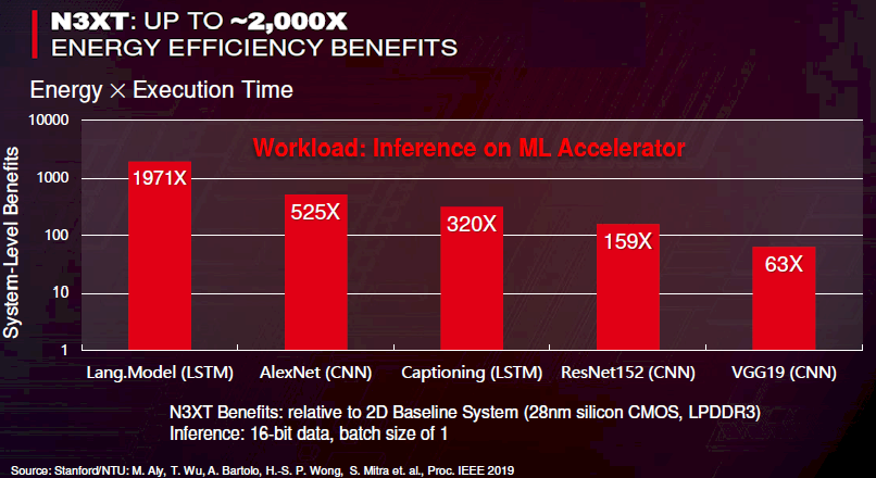
The advantage of the N3XT over two-dimensional systems
It sounds promising. But Wong did not spread how exactly these technologies in the next 30 years will be able to maintain the speed of technology improvement necessary for Moore’s law. For example, the transition to new nanomaterials will give us a one-time increase in the density of transistors with respect to two-dimensional components. But even there, in the end, we will encounter atomic restrictions.
Theoretically, if you can double the height of three-dimensional devices every 18 months, you can achieve an increase in density per square surface area. Of course, for mobile and embedded devices, this approach will quickly become too cumbersome, and the chips for computers in data centers after seven to eight generations will rest in a 4-meter ceiling.
In order for everything to continue to work for several decades, and the density continued to fit into the curve of Moore's law, it would be necessary to develop other technical innovations not mentioned by Wong. But if you produce chips like TSMC, you have to accept that researchers will constantly give you new candidates for technologies that need only requests from new, more demanding tasks to enter the market. And if you recall the story, then such tasks will certainly appear.
All Articles