Light control: a new type of optical elements based on metamaterials
Every day we are faced with processes and phenomena that we do not even notice, or rather, do not even see. Some of them we understand, and some we only have to understand. But the work of the scientific community was never limited to understanding anything, because a person always wanted to not only understand, but put his knowledge into practice, and this most often means only one thing - control. Today we will meet with you a study in which scientists from the University of Washington were able to create a new metamaterial that can manipulate light on a nanometer scale. What are the features of their structure, what role did the work of Gustav Mi play in this, and what is the practical implementation of this innovation? We learn about this from the report of the research group. Go.
Study basis
The ancestors of this study are optical elements based on arrays of discrete dielectric scatterers that can control the local amplitude and phase of optical fields. Such developments have made it possible to miniaturize traditional optical elements such as lenses and retroreflectors. In addition, arrays of dielectric scatterers became the basis for new multifunctional optical elements based on polarization or wave multiplexing and point scattering functions.
At the moment, the vast majority of research in this area was carried out with an eye to intuitively oriented methods of direct design. Such methods realize the desired phase profile using precompiled discrete diffuser libraries. The properties of such scatterers are calculated taking into account periodic boundary conditions when it is assumed that one scatterer behaves in the same way as an array of scatterers. This approximation, commonly known as the local phase approximation, neglects the differences in the interactions between adjacent scatterers in the optical element, which is unacceptable for a phase profile with a steep gradient. In addition, in the absence of a known phase profile, this approach cannot be used to create an optical element.
Reverse engineering methods begin by determining the quality factor as a function of the adjustable parameters of the diffuser, which attempt to accurately encapsulate the characteristics of the optical element. That is, the algorithm calculates the quality factor and its gradient for a given configuration of dielectric scatterers, and does not select the configuration itself by trial and error. The algorithm then approaches the configuration, using the gradient as the updated direction to optimize the quality factor.
In this case, the reverse engineering method allows one to study those diffuser configurations that would be ignored by intuitive direct design methods.
The reverse engineering method has previously been successfully used in the creation of plasmon nanostructures and dielectric planar integrated photonic elements, as well as in the recent development of two-dimensional optical elements based on scatterers. The resulting devices showed an increased efficiency of beam deflection at a large angle and multilayer lenses.
However, due to the need for a large amount of memory and poor scalability for large systems consisting of small elements, reverse engineering methods can only be applied to two-dimensional elements or very small three-dimensional elementary cells.
Naturally, this did not stop scientists from the University of Washington, so they decided to try using the reverse engineering method in their research, but made some changes and additions. As a result, they managed to create PSF (point scattering functions) in three dimensions using the gradient-based reverse engineering method for arrays of spherical Mie scatterers.
Before diving into the abyss of research results, a little understanding of terminology.
Firstly, metamaterials. This term refers to complex systems whose properties are characterized not by the properties of the material of which they are composed, but by the structure of the system itself.
We all remember that a tray of 30 eggs can withstand considerable weight, but this does not mean the strength of the shell. The shell itself is not so strong, but the "egg tray" is our metamaterial - a system whose strength does not depend on the strength of the shell, but on the number of eggs and their position.
An example of a complex structure of metamaterials.
A similar example would be a cardboard box with many partitions inside (like a grill). The fact that such a box can withstand heavy weight does not mean the strength of the cardboard, but is only a consequence of the specific structure of the box, i.e. a consequence of the presence of partitions.
Secondly, the scattering of Mi. Gustav Mi (1868-1957) is a German physicist who has been actively and successfully studying and explaining electrodynamics and theory of relativity. It is best known for its solution of the Maxwell equation - the scattering of light by a spherical particle.
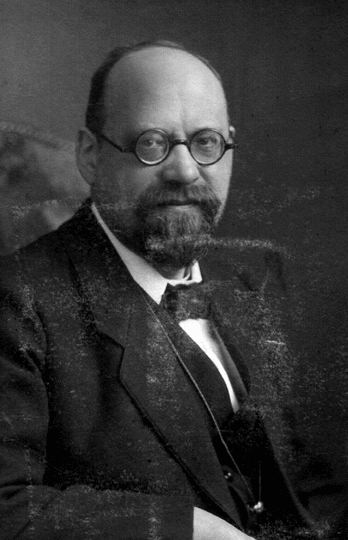
Gustav Mi
The essence of his decision is in relation to the particle size and the wavelength that falls on this particle. There are three scenarios: a particle is much smaller than a wavelength, they are about the same and a particle is much larger than a wavelength.
In the first case, we obtain Rayleigh scattering, that is, scattering without changing the wavelength of the particles. In this situation, the particle is polarized by an external electromagnetic wave, which leads to the excitation of an alternating dipole, which oscillates in time with the frequency of the external wave. Thus, we obtain a directivity diagram of the light that is characteristic of the dipole moment.
In the second case, the directivity pattern is complicated, because there are interference waves (mutual increase / decrease in the amplitude of several waves when they are superimposed on each other) reflected from different points on the particle surface.
In the third case, when the particle prevails in size, its surface will behave like a plane, due to which refraction and reflection of light will occur.
Research results
In their work, scientists prepared and tested in practice optical elements for wavelengths of 1.55 and 3 microns. The dimensions of the studied systems were 114 x 114 microns and 200 x 200 microns. Systems of this size, as the researchers themselves say, are record-breaking for those that were developed using reverse engineering.
The intensity profile for all tested devices with both wavelengths was set as a discrete spiral defined by eight focal points along the optical axis. Each of these points is located in a separate focal plane, divided along the optical axis by 28 μm for a wavelength of 1.55 μm and 57 μm a wavelength of 3 μm. Focal points are located on circles with a radius of 12 μm for a wavelength of 1.55 and 20 μm for a wavelength of 3 μm.
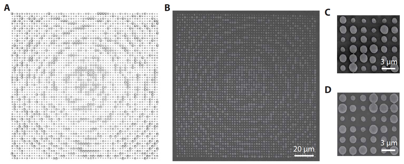
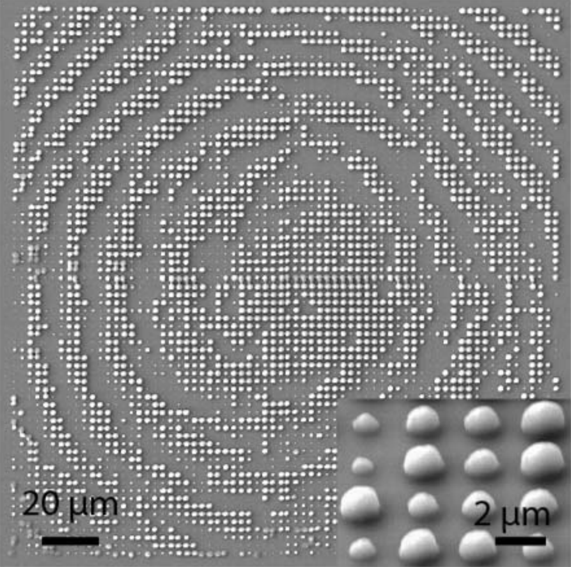
Image No. 1: A - schematic representation of the location of the spheres, B - SEM image 1.55 μm of the device coated with gold, C and D - production errors on the device.
* SEM - scanning electron microscope.For the manufacture of devices, a two-photon lithographic system was used. During the manufacturing process, we used a 63x lens paired with an IP-Dip resistor (n ~ 1.47 at the calculated wavelengths), which gives the maximum possible resolution during manufacturing (~ 200 nm).
The main task at the manufacturing stage is to create a set of identical spheres on a square grid in a vacuum. The substrate was not used, since its effect on the performance of the device was extremely negligible.
The spherical frequency for a device with a wavelength of 1.55 μm was set to 2.42 μm (superwave), and for a device with a wavelength of 3 μm, 2.9 μm (subwave).
As we can see in the pictures 1C and 1D , not all spheres are spheres, i.e. some of them are irregular in shape. Such production errors were not taken into account in modeling and optimization.
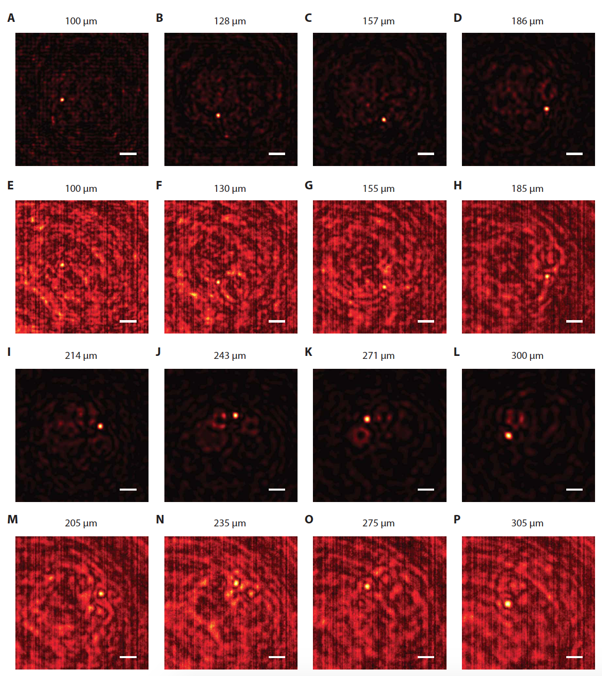
Image No. 2: operation of a 1.55 micron device during simulation and during actual tests.
During testing, two separate microscopes were used for each device (1.55 and 3 μm). During the experiments, it was found that the optical element creates a clear spot (point) of high intensity, which corresponds to the modeling predictions. However, the experiment shows a lower contrast between the focal point and the background compared to the simulation. In addition, in pictures 2E , 2F, and 2N , smaller hot spots of significant intensity are clearly visible, which were not present in the simulation.
Actual focal points are created at the correct spatial location on the plane, however there is a slight offset between the expected focal point positions along the optical axis for the focal points shown on 2M and 2N . Scientists explain these discrepancies in modeling and experiments with production errors.
Next, a comparison was made of the location of focal points in the plane during simulation and during experiments. The simulated (red) dots shown in 3A lie on a dashed black circle with a radius of 12 μm.
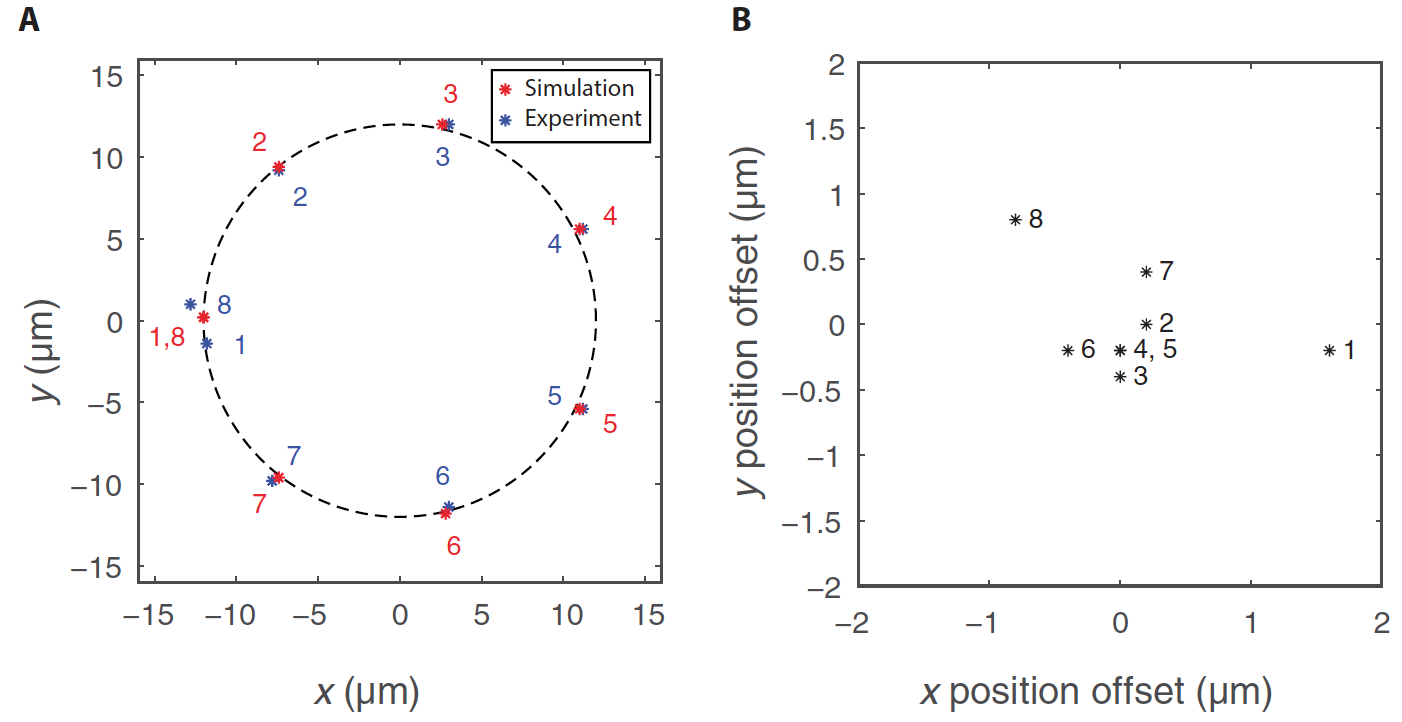
Image No. 3: A - the location of the focal points, B - the difference in the position of the simulated and experimental points.
The experimental (blue) dots adhere to a large extent to the same shape and behavior corresponding to a given Q factor. Nevertheless, there are some errors - the first and last points do not lie perfectly on each other (1 and 8 in image 3A ). Such discrepancies can be associated both with errors during production and with errors during optical characterization.
This technique is not without problems. The main disadvantage at the moment should be considered limited exclusively by spherical scatterers and a low refractive index. Mie scattering can be combined with the theory of T-matrices, which allows the use of particles of arbitrary shape (cylinders, ellipsoids, etc.). In particular, the combination of the studied method with cylindrical scatterers would make it possible to apply this method to classical processes for the production of binary semiconductors. In addition, the application of the theory of T-matrices will improve the refractive indices, which are an important component of the degree of performance of an optical element.
For a more detailed acquaintance with the nuances of the study, I recommend that you look into the report of scientists and additional materials to it.
Epilogue
In this study, scientists were able to successfully demonstrate in practice a design method using Mie backscattering, which allows you to set optical fields in three dimensions and is well suited for large arrays of discrete dielectric scatterers. This method allows the most efficient use of the properties of individual diffusers for the benefit of a common system for them.
During the experiments, scientists tested this method by developing an optical element that creates a discrete spiral optical focusing diagram. Such an element, creating a lens-like PSF, can be used in visualization systems associated with the extraction of elements on certain depth planes without performing a deconvolution operation.
This work is the first step towards the realization of the idea of “flexible” optics, when it is possible to create optical elements whose properties will be ideally suited for specific tasks.
Thank you for your attention, remain curious and have a good working week, guys! :)
Thank you for staying with us. Do you like our articles? Want to see more interesting materials? Support us by placing an order or recommending it to your friends, a 30% discount for Habr users on a unique analogue of entry-level servers that was invented by us for you: The whole truth about VPS (KVM) E5-2650 v4 (6 Cores) 10GB DDR4 240GB SSD 1Gbps from $ 20 or how to divide the server? (options are available with RAID1 and RAID10, up to 24 cores and up to 40GB DDR4).
Dell R730xd 2 times cheaper? Only we have 2 x Intel TetraDeca-Core Xeon 2x E5-2697v3 2.6GHz 14C 64GB DDR4 4x960GB SSD 1Gbps 100 TV from $ 199 in the Netherlands! Dell R420 - 2x E5-2430 2.2Ghz 6C 128GB DDR3 2x960GB SSD 1Gbps 100TB - from $ 99! Read about How to Build Infrastructure Bldg. class c using Dell R730xd E5-2650 v4 servers costing 9,000 euros for a penny?
All Articles