Speeding up a program for a Redd synthesized processor without optimization: replacing a clock
Until now, we have been discussing the topic of how to increase the system’s speed using some intensive methods. But in fact, there are extensive methods. Now we are working at a clock frequency of 50 MHz, which is associated with the use of a component from the set for a university program (and without it it is impossible to clock SDRAM, which requires that the clock pulses going to the microcircuit be shifted relative to the main ones). When I introduced this component to the game, I warned that this solution is temporary. Then I dumped so much new information on the reader that any extra tediousness could lead to an exclamation: “Well, these FPGAs, everything is so complicated here!” Now we are already easily and naturally constructing processor systems, all the terrible things are behind us. It's time to figure out how you can make your own component, which allows you to increase the clock frequency of both the processor and the peripherals connected to it.
Let's estimate what frequency we can painlessly set for the clocking of all our iron. The SDRAM chip used in the complex allows a limit frequency of 133 MHz. For processor clock speeds, see the Nios II Performance Benchmarks . There, for our FPGA Cyclone IV E, the Nios II / f core frequency of 160 MHz is guaranteed. I am not a supporter of squeezing all the juices out of the system, so we will talk about working at a frequency of 100 MHz.
To be honest, I still have not imbued with the methodology for calculating the shift of the clock frequency given in section 32.7. Clock, PLL and Timing Considerations of the Embedded Peripherals IP User Guide , but it seems like I'm not the only one. At least, a long search on the net did not lead me to articles that would contain any results calculated in the same way, but not for the frequency that is given in the main document (the same 50 MHz).
There is an interesting article to which I will give a direct link www.emb4fun.de/fpga/nutos1/index.html . One could just refer to it and say “Let's do as the author”, if not for one “but”: the author of this article uses the PLL block (in Russian - PLL, and at the household level - a frequency converter), inserting its own code in VHDL. I, as already noted in the article about the fun Quartusel , adhere to the ideology that the processor system should be at the top level of the project hierarchy. No insertions are needed in any language, be it VHDL or Verilog. Recently, this approach of mine has received one more confirmation: we have a new employee, a student who does not speak Verilog yet, but makes code for the Redd complex perfectly, since the chosen approach allows this.
It turns out that we just take as a basis that everything works for the author with a shift of minus 54 degrees (what kind of degrees is described in the article, the link to which I gave the paragraph above).
Next, pay attention to another interesting article asral.unimap.edu.my/wp-content/uploads/2019/07/2019_IJEECS_Chan_Implementation-Camera-System.pdf . Everything works for authors at a shift of minus 65 degrees.
Let's try to make our system using a value from this range. If during the daily test of RAM there is not a single malfunction, then we will leave this value as combat. We have the right, since the developed “firmware” for Redd will not go to the Customers, but will be used for internal needs, and in piece quantities. If anything, it will always be possible to fix everything without unnecessary difficulties (difficulties arise when it is necessary to update the “firmware” in thousands of devices sold, and simply at the remote Customer).
For some reason, it seems to me that the processor system for this article is easier to do from scratch than to remake from the old one. Just how to demonstrate the “twist, twist, I want to confuse” process, constantly referring to past articles, I'd rather show it all again from the very beginning. At the same time, we fix the material. So, let's get started.
At the very beginning, we are shown a completely empty system containing only a clock and reset signal source.
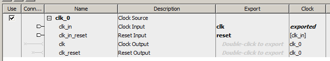
Usually I don’t change anything there, but today I will make an exception. I don’t want to be distracted by the reset circuit, since we will still work from under the debugger. Therefore, I will switch the reset condition from the level to a negative difference, and the leg itself will subsequently be nullified.
But here the clock signal has a frequency of 50 MHz (this frequency is set by the characteristics of the generator soldered to the board). In the first of the articles I mentioned above, the PLL block added to the main project was used. Where do we get it here? And here he is!
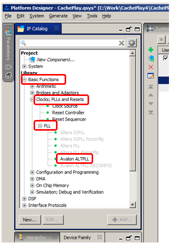
This is the same block, but here we do not have to embed any code in the Verilog or VHDL languages. Everything is already inserted for us! True, the settings for different types of FPGAs differ slightly more than completely. More precisely, the tunable parameters are more or less the same, but they are located in fundamentally different places in the configuration dialogs. Since the Cyclone IV E FPGA is used in the Redd complex, we will consider the configuration of this option.
On the first tab, we replace the input frequency with 50 MHz (by default it was 100) and go to the next tab (click Next, for Cyclone IV E we have to do this many times).

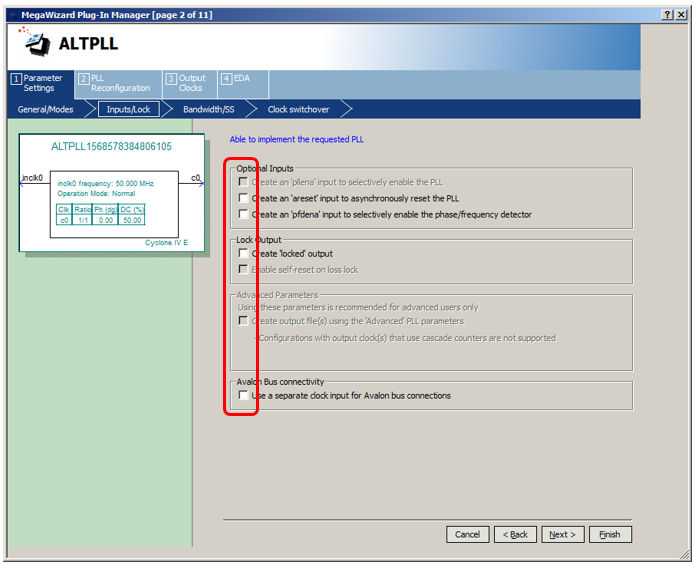
Uncheck the additional inputs and outputs. We do not need them:
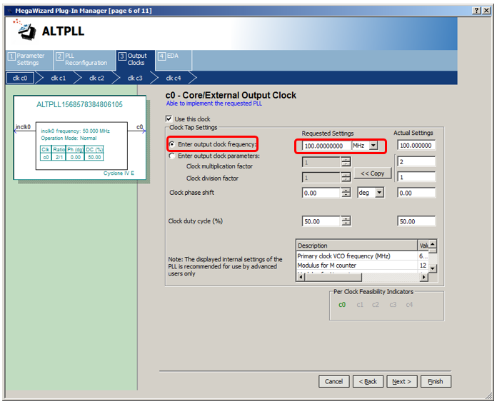
We skip the next few tabs until we get to setting the output C0. There we switch the radio button to set the frequency and enter the value of 100 MHz:
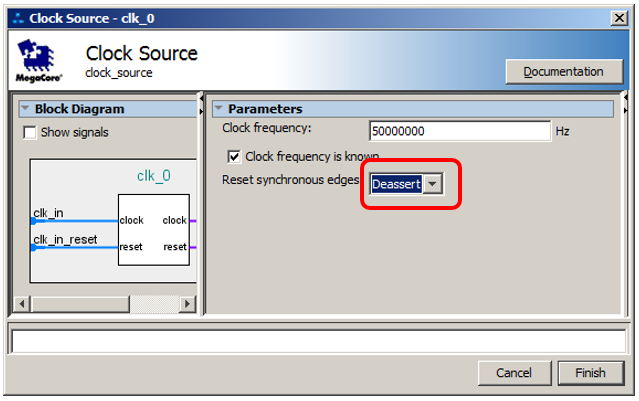
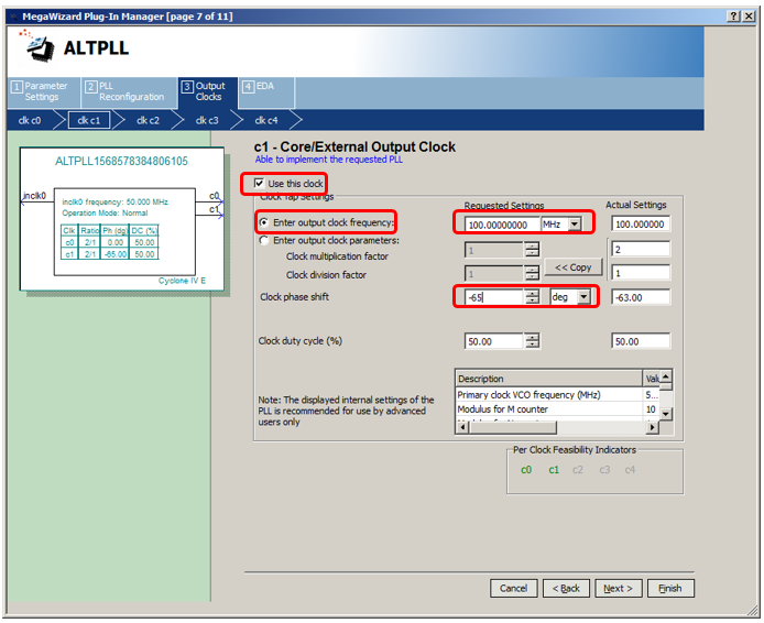
With C1, things are a little more complicated. First, select the checkbox saying that it should also be used. Secondly, we similarly set the frequency of 100 MHz. Well, and thirdly, we set the frequency shift. Which one to ask? Minus 58 or minus 65? Of course, I tried both options. Both have earned me. But the argument on the topic minus 58 looks a little less convincing, so here I will recommend to enter the value minus 65 degrees (while automation will tell me that the actual value achieved will be minus 63 degrees).
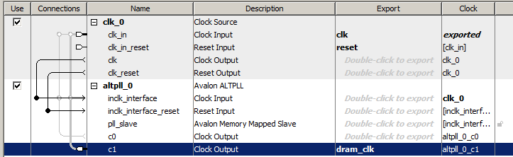
Well, that’s it. Now you can step through the Next button to the end, or you can just click Finish . We connect the inputs inclk_interface and inclk_interface_reset . The output c0 will be used as a clock for the entire system. The output c1 is exported for clocking the sdram chip. In the future, you will need to remember to connect the data bus to the pll_slave input. For Cyclone V, this would not be necessary.
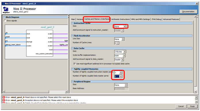
Add a processor core. Today, our SDRAM will be subject to testing. So, the code should not be located in it. And this, in turn, means that all the code will be located in the internal RAM of the FPGA. That is, we do not need an instruction cache. Turn it off, saving FPGA memory. We also connect via one highly connected bus of instructions and data. No more interesting settings for the processor core are required.
With the usual movement of the hand, add two blocks of internal RAM FPGA. One is a dual port with a capacity of 16 kilobytes and one is a single port with a capacity of 4 kilobytes. How to name them and how to connect, I hope everyone remembers. Last time I liked to highlight the tires with flowers, perhaps for ease of reading, I will do so in this article.
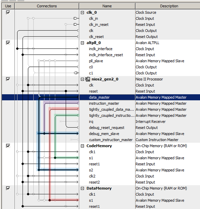
Do not forget to assign these memory blocks special addresses in the personal range and lock them. Let CodeMemory be assigned to 0x20000000, and DataMemory to 0x20004000.
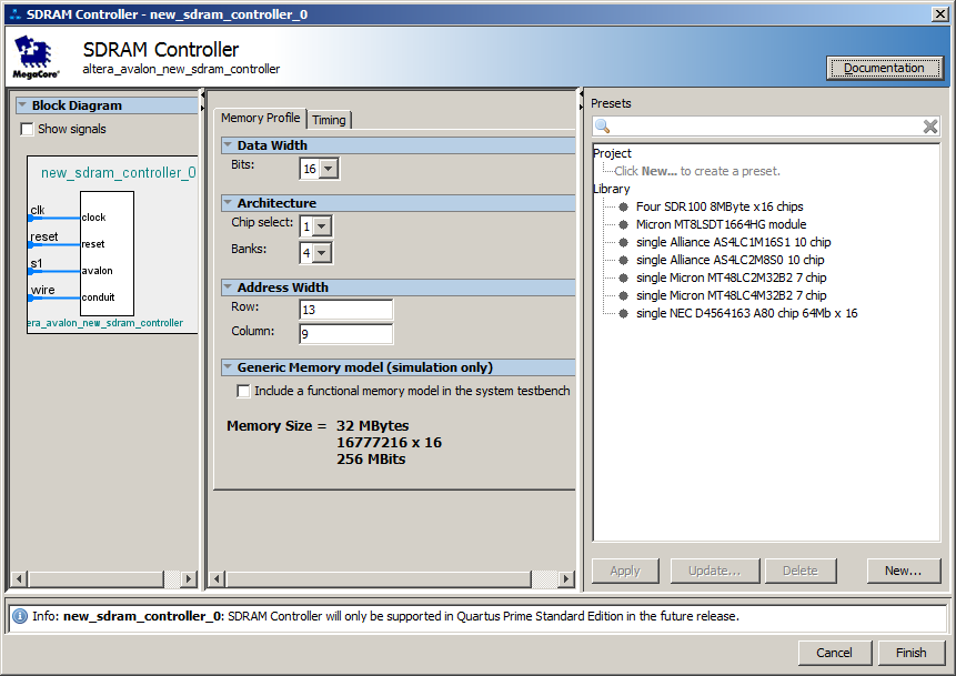
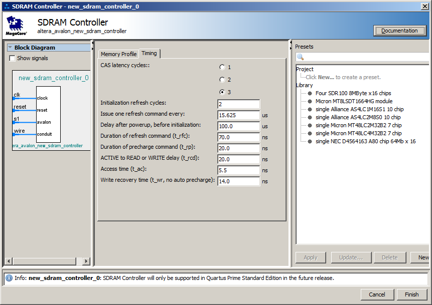
Well, let's add an SDRAM block to the system, setting it up, as well as JTAG-UART blocks for outputting messages and a single-bit GPIO , on which we will measure the real frequency to make sure that it increases. For reference, here are some non-obvious settings:

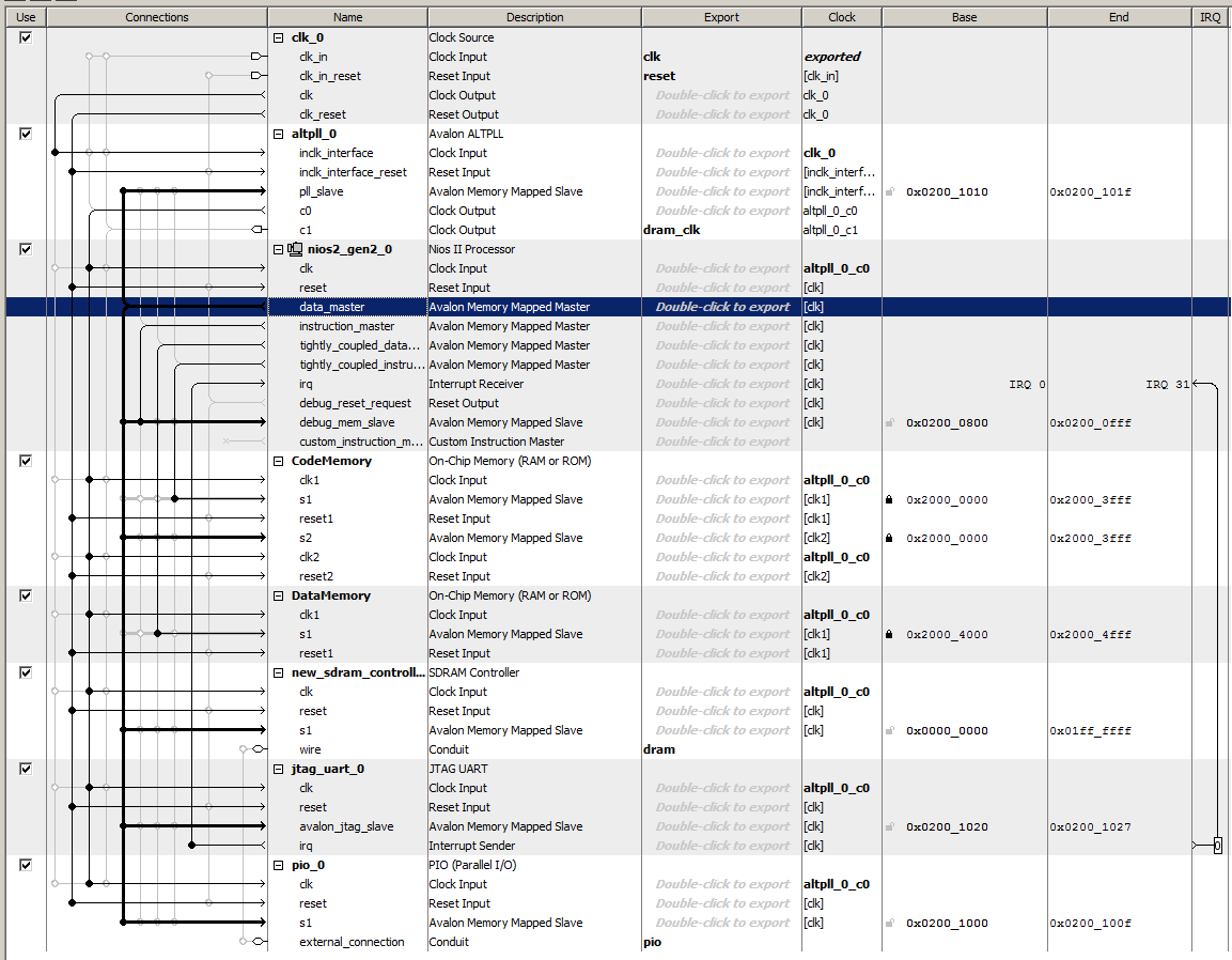
In total, we get such a system (I highlighted the data bus, since it scans across all external devices):
We assign vectors to the processor, automatically assign addresses, automatically assign interrupt numbers, to the generating system.
We connect the system to the project, do a rough assembly, assign the leg numbers, and this time we make virtual not only CKE , but also reset_n (how to do this, I told you in one of the previous articles , look for Virtual Pin there). We make the final assembly, fill the equipment in the FPGA. All. We’ve finished the equipment, go to the software part.
For a change, let's create a project based on a template not of Hello World Small , but of Memory Test Small :
When it was created, go to the BSP editor. As usual, the first thing we do is turn off the SysID check and allow the use of C ++ (though this time I won’t change the file type, but it’s already a habit for me):
But the most important thing we have to fix on the Linker Script tab. Automation recognized that the instruction bus only goes to CodeMemory , so it placed a section of code (called .text ) in CodeMemory . But taking care of us, she placed everything else in the largest data region, which is located in SDRAM . How did she know that we would mercilessly erase this memory?

We will have to manually, line by line, replace the region with DataMemory (selection lists will appear there, the selection should be rearranged in them). We should get this picture:
We exit the editor, generate the BSP, try to run the program for debugging. We get the following text:
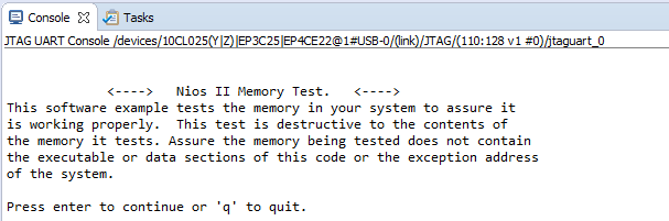
If I press Enter, I didn’t succeed. I entered something (yes even a space) and then pressed Enter. Then they asked me:

Hour by hour is not easier. And what address to enter? You can open Platform Designer and see the value there. But I usually look in the universal reference file system.h (the full path for my project is C: \ Work \ CachePlay5 \ software \ MemoryTest_bsp \ system.h). There we are interested in two lines:
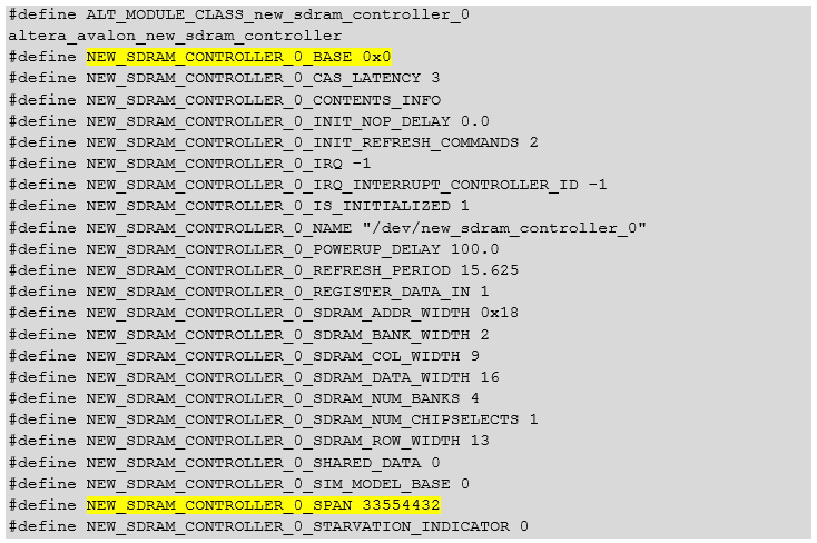
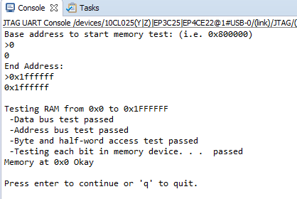
where decimal 33554432 is equal to hex 0x2000000. Therefore, my answers and the result should look like this:
Great, but this is not good for a daily test. I rewrote the main function like this:
The dots indicate that the program did not “freeze”. If there is an error, an asterisk will be displayed. For reliability, you can put a breakpoint on its output, then just do not sleep it.
True, the "left" points climbed from somewhere. It turned out that they are displayed inside the MemTestDevice () function. There I erased their conclusion. The test was successful. The resulting system can be used, at least for internal needs (namely, such developments are carried out under the Redd complex).
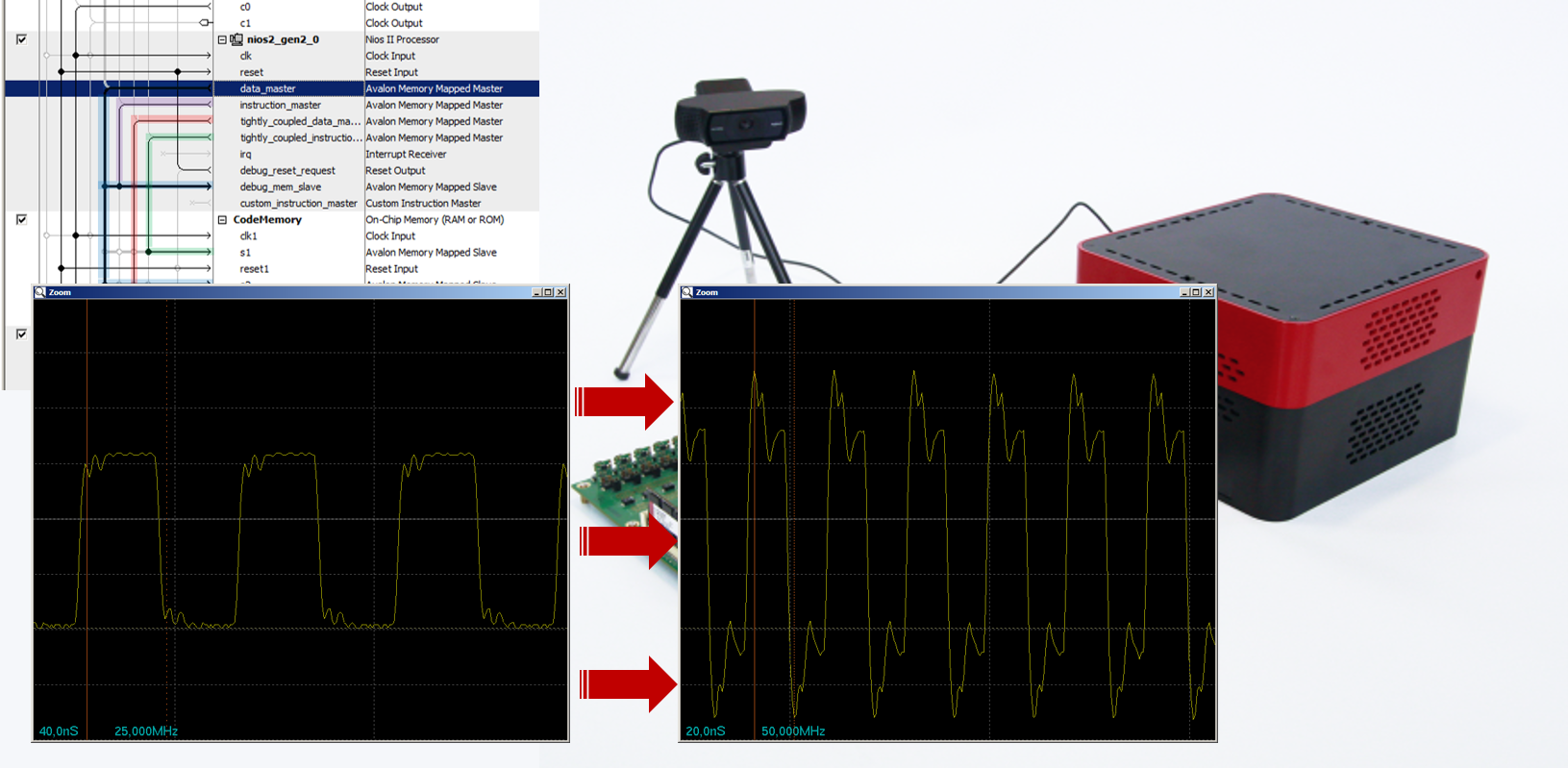
But I’m already used to the fact that when working with equipment you can’t trust anything. Everything should be checked carefully. Let's make sure that we work at a frequency doubled compared to previous articles. Add the well-known function MagicFunction1 ().
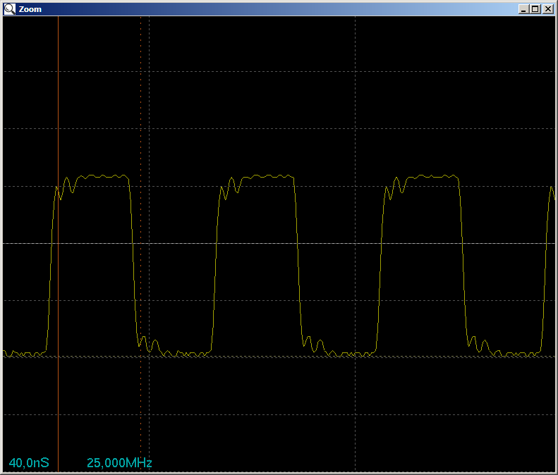
We will call it from main () , we will catch the pulses on the oscilloscope, but this time we will pay attention not only to their beauty, but also to the frequency (let me remind you that each drop at least up, even down is one command, so you can measure the distance between the drops )
Only 50 megahertz. Has the frequency really not increased? Compare with the frequency from the code developed when writing the last article, and we understand that everything is in order. It’s just that the regular pio unit requires 2 clock cycles per output to the port (in a home-made one I got 1 clock, but here it’s enough for us to make sure that the system’s performance has doubled).
We learned how to use a custom PLL block instead of a fixed clock generator. True, the detected constants are designed for a frequency of 100 MHz, but everyone can adjust them to any other frequency either using well-known calculations, or by trial and error. We also strengthened the skills of creating an optimal processor system and made sure that the memory at a higher frequency works stably, and the frequency really increased.
In general, we can already produce any computing things, we can even exchange with the central processor, but the central processor of the complex will cope with the banal calculations more efficiently. FPGA is added to Redd in order to implement any high-speed interfaces or capture (well, or play) information flows. We have already mastered the basics of designing, we have learned how to provide more or less high performance. It's time to continue working with interfaces, which is what we will do in the next article. More precisely, a set of articles, mindful of the rule "one article - one thing."
Previous articles in the series:
- Development of the simplest “firmware” for FPGAs installed in Redd, and debugging using the memory test as an example.
- Development of the simplest “firmware” for FPGAs installed in Redd. Part 2. Program code.
- Development of its own core for embedding in a FPGA-based processor system.
- Development of programs for the central processor Redd on the example of access to the FPGA.
- The first experiments using the streaming protocol on the example of the CPU and processor communication in the FPGA of the Redd complex.
- Merry Quartusel, or how the processor has come to such a life.
- Code Optimization Methods for Redd. Part 1: cache effect.
- Code Optimization Methods for Redd. Part 2: non-cached memory and parallel bus operation.
A bit of theoretical reasoning
Let's estimate what frequency we can painlessly set for the clocking of all our iron. The SDRAM chip used in the complex allows a limit frequency of 133 MHz. For processor clock speeds, see the Nios II Performance Benchmarks . There, for our FPGA Cyclone IV E, the Nios II / f core frequency of 160 MHz is guaranteed. I am not a supporter of squeezing all the juices out of the system, so we will talk about working at a frequency of 100 MHz.
To be honest, I still have not imbued with the methodology for calculating the shift of the clock frequency given in section 32.7. Clock, PLL and Timing Considerations of the Embedded Peripherals IP User Guide , but it seems like I'm not the only one. At least, a long search on the net did not lead me to articles that would contain any results calculated in the same way, but not for the frequency that is given in the main document (the same 50 MHz).
There is an interesting article to which I will give a direct link www.emb4fun.de/fpga/nutos1/index.html . One could just refer to it and say “Let's do as the author”, if not for one “but”: the author of this article uses the PLL block (in Russian - PLL, and at the household level - a frequency converter), inserting its own code in VHDL. I, as already noted in the article about the fun Quartusel , adhere to the ideology that the processor system should be at the top level of the project hierarchy. No insertions are needed in any language, be it VHDL or Verilog. Recently, this approach of mine has received one more confirmation: we have a new employee, a student who does not speak Verilog yet, but makes code for the Redd complex perfectly, since the chosen approach allows this.
It turns out that we just take as a basis that everything works for the author with a shift of minus 54 degrees (what kind of degrees is described in the article, the link to which I gave the paragraph above).
Next, pay attention to another interesting article asral.unimap.edu.my/wp-content/uploads/2019/07/2019_IJEECS_Chan_Implementation-Camera-System.pdf . Everything works for authors at a shift of minus 65 degrees.
Let's try to make our system using a value from this range. If during the daily test of RAM there is not a single malfunction, then we will leave this value as combat. We have the right, since the developed “firmware” for Redd will not go to the Customers, but will be used for internal needs, and in piece quantities. If anything, it will always be possible to fix everything without unnecessary difficulties (difficulties arise when it is necessary to update the “firmware” in thousands of devices sold, and simply at the remote Customer).
New piece of hardware configuration
For some reason, it seems to me that the processor system for this article is easier to do from scratch than to remake from the old one. Just how to demonstrate the “twist, twist, I want to confuse” process, constantly referring to past articles, I'd rather show it all again from the very beginning. At the same time, we fix the material. So, let's get started.
At the very beginning, we are shown a completely empty system containing only a clock and reset signal source.
Usually I don’t change anything there, but today I will make an exception. I don’t want to be distracted by the reset circuit, since we will still work from under the debugger. Therefore, I will switch the reset condition from the level to a negative difference, and the leg itself will subsequently be nullified.
But here the clock signal has a frequency of 50 MHz (this frequency is set by the characteristics of the generator soldered to the board). In the first of the articles I mentioned above, the PLL block added to the main project was used. Where do we get it here? And here he is!
This is the same block, but here we do not have to embed any code in the Verilog or VHDL languages. Everything is already inserted for us! True, the settings for different types of FPGAs differ slightly more than completely. More precisely, the tunable parameters are more or less the same, but they are located in fundamentally different places in the configuration dialogs. Since the Cyclone IV E FPGA is used in the Redd complex, we will consider the configuration of this option.
On the first tab, we replace the input frequency with 50 MHz (by default it was 100) and go to the next tab (click Next, for Cyclone IV E we have to do this many times).
Uncheck the additional inputs and outputs. We do not need them:
We skip the next few tabs until we get to setting the output C0. There we switch the radio button to set the frequency and enter the value of 100 MHz:
With C1, things are a little more complicated. First, select the checkbox saying that it should also be used. Secondly, we similarly set the frequency of 100 MHz. Well, and thirdly, we set the frequency shift. Which one to ask? Minus 58 or minus 65? Of course, I tried both options. Both have earned me. But the argument on the topic minus 58 looks a little less convincing, so here I will recommend to enter the value minus 65 degrees (while automation will tell me that the actual value achieved will be minus 63 degrees).
Well, that’s it. Now you can step through the Next button to the end, or you can just click Finish . We connect the inputs inclk_interface and inclk_interface_reset . The output c0 will be used as a clock for the entire system. The output c1 is exported for clocking the sdram chip. In the future, you will need to remember to connect the data bus to the pll_slave input. For Cyclone V, this would not be necessary.
Other hardware parts, purely for fixing material
Add a processor core. Today, our SDRAM will be subject to testing. So, the code should not be located in it. And this, in turn, means that all the code will be located in the internal RAM of the FPGA. That is, we do not need an instruction cache. Turn it off, saving FPGA memory. We also connect via one highly connected bus of instructions and data. No more interesting settings for the processor core are required.
With the usual movement of the hand, add two blocks of internal RAM FPGA. One is a dual port with a capacity of 16 kilobytes and one is a single port with a capacity of 4 kilobytes. How to name them and how to connect, I hope everyone remembers. Last time I liked to highlight the tires with flowers, perhaps for ease of reading, I will do so in this article.
Do not forget to assign these memory blocks special addresses in the personal range and lock them. Let CodeMemory be assigned to 0x20000000, and DataMemory to 0x20004000.
Well, let's add an SDRAM block to the system, setting it up, as well as JTAG-UART blocks for outputting messages and a single-bit GPIO , on which we will measure the real frequency to make sure that it increases. For reference, here are some non-obvious settings:
In total, we get such a system (I highlighted the data bus, since it scans across all external devices):
We assign vectors to the processor, automatically assign addresses, automatically assign interrupt numbers, to the generating system.
We connect the system to the project, do a rough assembly, assign the leg numbers, and this time we make virtual not only CKE , but also reset_n (how to do this, I told you in one of the previous articles , look for Virtual Pin there). We make the final assembly, fill the equipment in the FPGA. All. We’ve finished the equipment, go to the software part.
We set up BSP for our environment
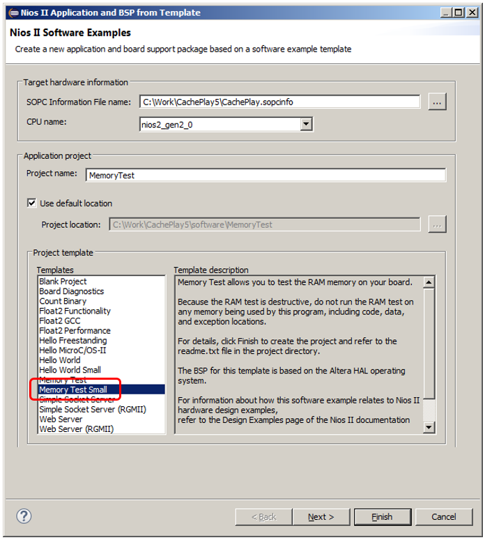
For a change, let's create a project based on a template not of Hello World Small , but of Memory Test Small :
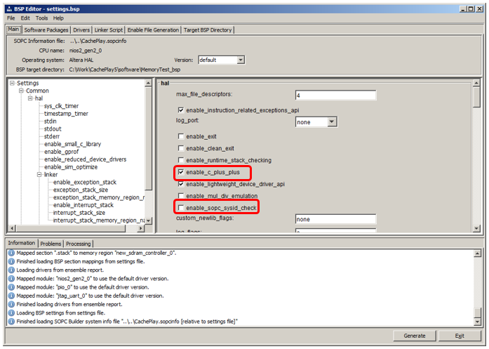
When it was created, go to the BSP editor. As usual, the first thing we do is turn off the SysID check and allow the use of C ++ (though this time I won’t change the file type, but it’s already a habit for me):
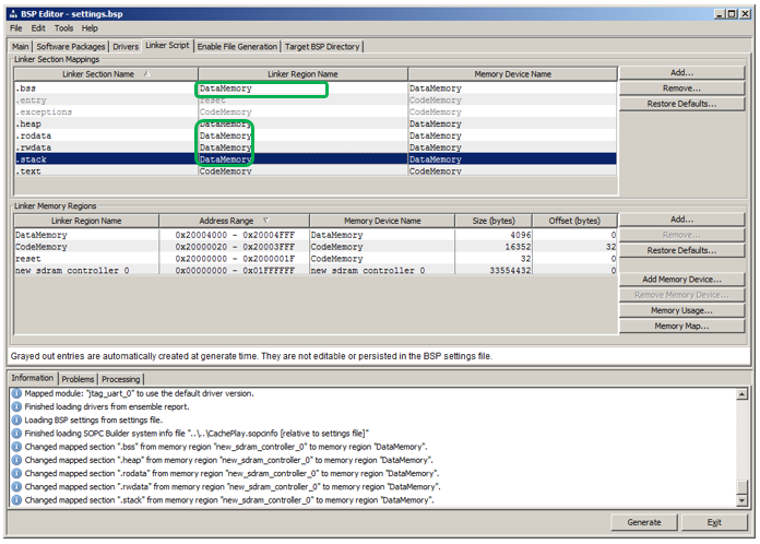
But the most important thing we have to fix on the Linker Script tab. Automation recognized that the instruction bus only goes to CodeMemory , so it placed a section of code (called .text ) in CodeMemory . But taking care of us, she placed everything else in the largest data region, which is located in SDRAM . How did she know that we would mercilessly erase this memory?
We will have to manually, line by line, replace the region with DataMemory (selection lists will appear there, the selection should be rearranged in them). We should get this picture:
Program Experiments
We exit the editor, generate the BSP, try to run the program for debugging. We get the following text:
If I press Enter, I didn’t succeed. I entered something (yes even a space) and then pressed Enter. Then they asked me:
Hour by hour is not easier. And what address to enter? You can open Platform Designer and see the value there. But I usually look in the universal reference file system.h (the full path for my project is C: \ Work \ CachePlay5 \ software \ MemoryTest_bsp \ system.h). There we are interested in two lines:
Same text
#define ALT_MODULE_CLASS_new_sdram_controller_0 altera_avalon_new_sdram_controller #define NEW_SDRAM_CONTROLLER_0_BASE 0x0 #define NEW_SDRAM_CONTROLLER_0_CAS_LATENCY 3 #define NEW_SDRAM_CONTROLLER_0_CONTENTS_INFO #define NEW_SDRAM_CONTROLLER_0_INIT_NOP_DELAY 0.0 #define NEW_SDRAM_CONTROLLER_0_INIT_REFRESH_COMMANDS 2 #define NEW_SDRAM_CONTROLLER_0_IRQ -1 #define NEW_SDRAM_CONTROLLER_0_IRQ_INTERRUPT_CONTROLLER_ID -1 #define NEW_SDRAM_CONTROLLER_0_IS_INITIALIZED 1 #define NEW_SDRAM_CONTROLLER_0_NAME "/dev/new_sdram_controller_0" #define NEW_SDRAM_CONTROLLER_0_POWERUP_DELAY 100.0 #define NEW_SDRAM_CONTROLLER_0_REFRESH_PERIOD 15.625 #define NEW_SDRAM_CONTROLLER_0_REGISTER_DATA_IN 1 #define NEW_SDRAM_CONTROLLER_0_SDRAM_ADDR_WIDTH 0x18 #define NEW_SDRAM_CONTROLLER_0_SDRAM_BANK_WIDTH 2 #define NEW_SDRAM_CONTROLLER_0_SDRAM_COL_WIDTH 9 #define NEW_SDRAM_CONTROLLER_0_SDRAM_DATA_WIDTH 16 #define NEW_SDRAM_CONTROLLER_0_SDRAM_NUM_BANKS 4 #define NEW_SDRAM_CONTROLLER_0_SDRAM_NUM_CHIPSELECTS 1 #define NEW_SDRAM_CONTROLLER_0_SDRAM_ROW_WIDTH 13 #define NEW_SDRAM_CONTROLLER_0_SHARED_DATA 0 #define NEW_SDRAM_CONTROLLER_0_SIM_MODEL_BASE 0 #define NEW_SDRAM_CONTROLLER_0_SPAN 33554432 #define NEW_SDRAM_CONTROLLER_0_STARVATION_INDICATOR 0
where decimal 33554432 is equal to hex 0x2000000. Therefore, my answers and the result should look like this:
Great, but this is not good for a daily test. I rewrote the main function like this:
int main(void) { int step = 0; while (1) { if (step++%100 == 0) { alt_printf ("."); } if (MemTestDevice(NEW_SDRAM_CONTROLLER_0_BASE, NEW_SDRAM_CONTROLLER_0_SPAN)!=0) { printf ("*"); } } return (0); }
The dots indicate that the program did not “freeze”. If there is an error, an asterisk will be displayed. For reliability, you can put a breakpoint on its output, then just do not sleep it.
True, the "left" points climbed from somewhere. It turned out that they are displayed inside the MemTestDevice () function. There I erased their conclusion. The test was successful. The resulting system can be used, at least for internal needs (namely, such developments are carried out under the Redd complex).
Checking the total system performance
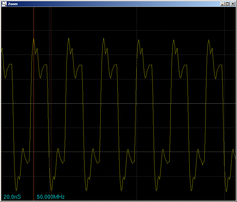
But I’m already used to the fact that when working with equipment you can’t trust anything. Everything should be checked carefully. Let's make sure that we work at a frequency doubled compared to previous articles. Add the well-known function MagicFunction1 ().
Let me remind you how she looks.
void MagicFunction1() { IOWR (PIO_0_BASE,0,1); IOWR (PIO_0_BASE,0,0); IOWR (PIO_0_BASE,0,1); IOWR (PIO_0_BASE,0,0); IOWR (PIO_0_BASE,0,1); IOWR (PIO_0_BASE,0,0); IOWR (PIO_0_BASE,0,1); IOWR (PIO_0_BASE,0,0); IOWR (PIO_0_BASE,0,1); IOWR (PIO_0_BASE,0,0); IOWR (PIO_0_BASE,0,1); IOWR (PIO_0_BASE,0,0); IOWR (PIO_0_BASE,0,1); IOWR (PIO_0_BASE,0,0); IOWR (PIO_0_BASE,0,1); IOWR (PIO_0_BASE,0,0); IOWR (PIO_0_BASE,0,1); IOWR (PIO_0_BASE,0,0); IOWR (PIO_0_BASE,0,1); IOWR (PIO_0_BASE,0,0); IOWR (PIO_0_BASE,0,1); IOWR (PIO_0_BASE,0,0); IOWR (PIO_0_BASE,0,1); IOWR (PIO_0_BASE,0,0); IOWR (PIO_0_BASE,0,1); IOWR (PIO_0_BASE,0,0); IOWR (PIO_0_BASE,0,1); IOWR (PIO_0_BASE,0,0); IOWR (PIO_0_BASE,0,1); IOWR (PIO_0_BASE,0,0); }
We will call it from main () , we will catch the pulses on the oscilloscope, but this time we will pay attention not only to their beauty, but also to the frequency (let me remind you that each drop at least up, even down is one command, so you can measure the distance between the drops )
Only 50 megahertz. Has the frequency really not increased? Compare with the frequency from the code developed when writing the last article, and we understand that everything is in order. It’s just that the regular pio unit requires 2 clock cycles per output to the port (in a home-made one I got 1 clock, but here it’s enough for us to make sure that the system’s performance has doubled).
Conclusion
We learned how to use a custom PLL block instead of a fixed clock generator. True, the detected constants are designed for a frequency of 100 MHz, but everyone can adjust them to any other frequency either using well-known calculations, or by trial and error. We also strengthened the skills of creating an optimal processor system and made sure that the memory at a higher frequency works stably, and the frequency really increased.
In general, we can already produce any computing things, we can even exchange with the central processor, but the central processor of the complex will cope with the banal calculations more efficiently. FPGA is added to Redd in order to implement any high-speed interfaces or capture (well, or play) information flows. We have already mastered the basics of designing, we have learned how to provide more or less high performance. It's time to continue working with interfaces, which is what we will do in the next article. More precisely, a set of articles, mindful of the rule "one article - one thing."
All Articles