Transition Metal Dichalcogenides: Unlocking the Secrets of WS2 Crystal Growth
“Well, have you tried? Now see the instructions. " This joke describes the reluctance of some people to first find out what and how to do according to the instructions, and only then proceed to work / assembly / installation. In the world of complex scientific research, discoveries and research, this also often happens, although not by the will of scientists. Some processes, the results of which are all clear and obvious to everyone, remain poorly investigated, which makes them difficult to improve. A prominent representative of such processes is the formation of transition metal dichalcogenides. However, nothing will be hidden from the curious gaze of scientists. So, scientists Toshiaki Kato and Toshiro Kaneko were able to personally observe the synthesis of transition metal dichalcogenides, which are semiconductor wafers with a thickness of several atoms. What is so unusual in these transition metal dichalcogenides, how did scientists discover their secrets and what does this mean for the semiconductor world? We learn about this from the report of the research group. Go.
Study basis
Transition metal dichalcogenides (hereinafter PDM) is a thin monolayer semiconductor consisting of a transition metal and chalcogen. One layer of metal atoms is located between two layers of chalcogen atoms, which can be expressed by the formula MX 2 (M - metal and X - chalcogen).
Chalcogenes include elements that are quite familiar to us: oxygen, sulfur, selenium, tellurium, polonium, and artificially synthesized liverworm (Lv).
The combination of these elements (metal and chalcogen) in the form of PDM in its structure is a two-dimensional material, due to its incredibly small thickness, which leads to the appearance of unusual properties and characteristics. Quite often, PDM is compared with graphene, another two-dimensional structure, the properties of which are very different from the properties of its three-dimensional base (carbon). A number of interesting properties of PDM include:
- MoS 2 , WS 2 , MoSe 2 , WSe 2 , MoTe 2 are direct-gap, i.e. in them, the transition of an electron from the conduction band to the valence band is not accompanied by a loss of momentum, which makes these compounds excellent for creating transistors in electronics or emitters and sensors in optics;
- PDMs do not have an inversion center * , which allows us to achieve a new degree of freedom of charge carriers $
- strong spin-orbit interaction in PDM monolayers leads to spin-orbit splitting of hundreds of meV in the valence band and several meV in the conduction band, which allows you to adjust the electron spin by adjusting the laser photon energy;
- the two-dimensionality of MoS 2 and the high spin-orbit coupling of this compound have great potential for spintronics.
The center of inversion * is the point inside the figure (the crystal in this case) at which any line drawn through it on either side of it and at equal distances will meet the corresponding points of the figure.And this is only a small part of the features inherent in PDM. And to expand this range of abilities can only be studied in more detail in the process of formation of PDM in different conditions. In the work we are considering today, scientists describe a new method for observing the dynamics of diffusion and nucleation during the growth of tungsten disulfide (WS 2 ). They also managed to accurately determine the diffusion length (L d ) of the precursor * .
Precursor * - a substance involved in the reaction of formation of the final substance.According to the study, the value of L d reached ~ 750 μm, which is almost two orders of magnitude higher than that of traditional semiconductors, such as Si 12 , GaAs 13 and SiC 14 . Scientists attribute such a large indicator to the precursor drops observed during the formation of WS 2 .
Research results
And now we will begin to consider what scientists were able to discover during their observations.
First of all, scientists note that to study the growth dynamics of two-dimensional crystals it is very useful to have control over the nucleation regions (the first stage of the phase transition). In their work, the researchers used point inclusions of gold (Au), which made it possible to precisely control the nucleation process WS 2 and the density of the nucleation regions ( 1a - 1c ).
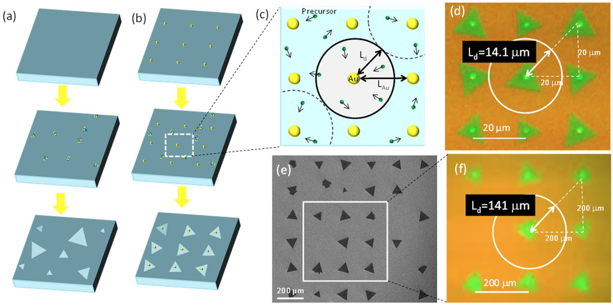
Image No. 1
Image 1d shows the results of the synthesis of WS 2 on a substrate containing an array of Au points, in which the distance between the centers of the Au points (L Au ) was 20 μm. The growth of triangular WS 2 crystals in regions with Au shows the presence of control over the nucleation regions and their density.
Next, the diffusion length (L d ), which is an important kinetic parameter of crystal growth ( 1c ), was experimentally determined. Considering that the growth of WS 2 was observed only in regions with Au, the SiO 2 substrate in the places between the Au points remained bare ( 1d ).
This observation allowed scientists to suggest two nucleation mechanisms. If almost all the precursor material delivered to the substrate from the vapor phase was effectively attracted by Au points and used for WS 2 growth, L d can be determined by the following formula:
L d ≈ √2L Au / 2
Interestingly, the formation of individual WS 2 crystals was observed only in Au regions even when L Au was ≤ 200 μm ( 1e and 1f ). And this suggests that the maximum indicator L d will not exceed 140 microns. This observation is also interesting in that the L d of conventional semiconductor materials (Si 12 , GaAs 13 and SiC 14 ) is in the range from 0.2 to 30 μm.
For a more accurate determination of L d and observation of the super-long diffusion of the precursor, diffusion barriers were established around the Au points ( 2a ).
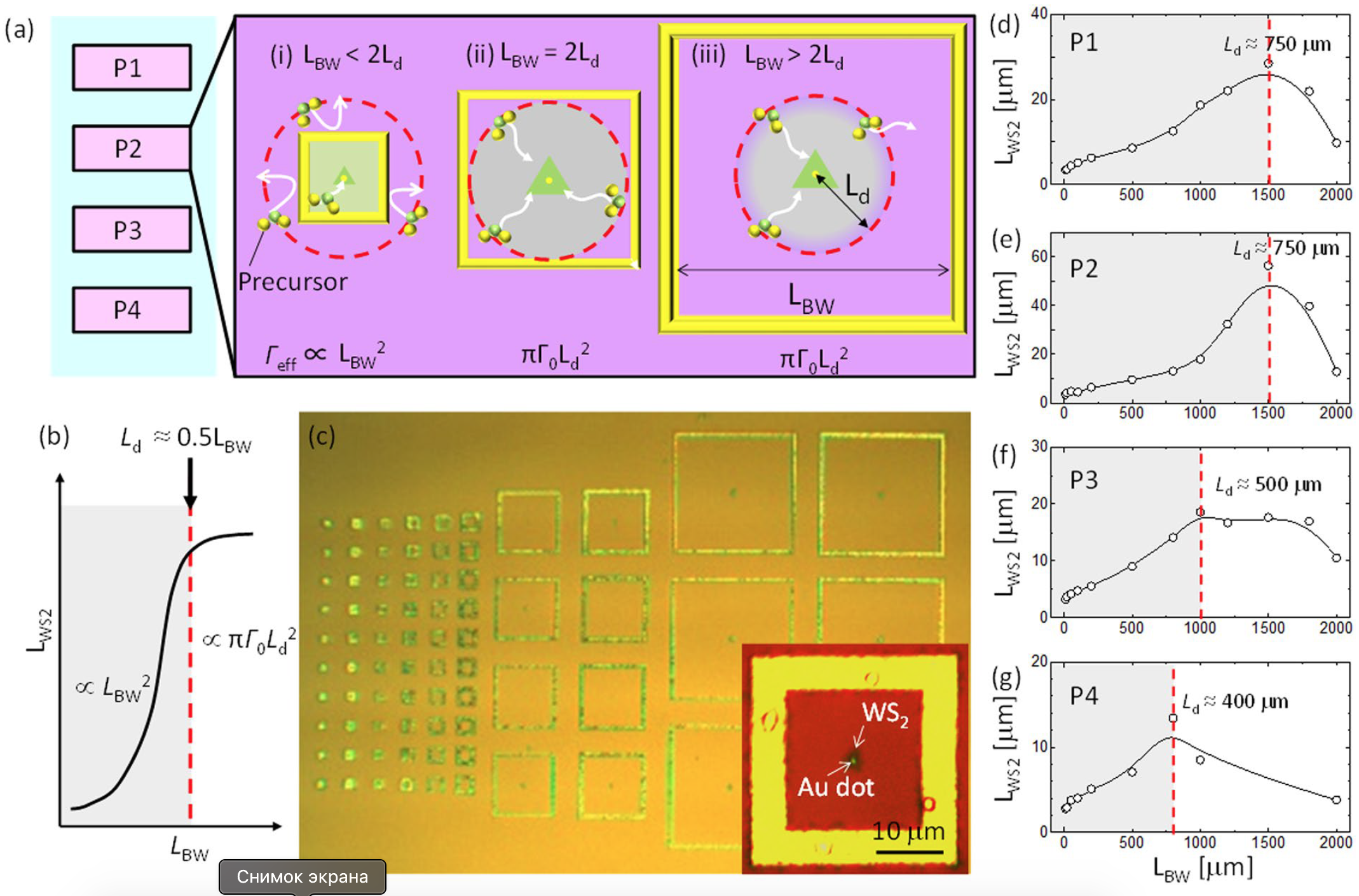
Image No. 2
Crystal growth stopped at the initial stage, when the length of each side of the triangular crystal WS 2 (L WS 2 ) increased with the growth time. The value of L WS 2 is very related to (Γ eff t) 0.5 in this model, where Γ eff is the effective precursor flux to the growth edge of WS 2 , and t is the growth time. Moreover, Γ eff was proportional to πΓ 0 L d 2 , where Γ 0 is the inflow of vapor-phase precursors to the substrate per unit area. Γ eff depends on the length of the diffusion barrier wall (L BW ); therefore, L WS 2 will vary depending on L BW ( 2a and 2b ).
Based on this model, scientists suggested a region in which the growth of L WS 2 will transition from the quadratic function L BW to the saturation state ( 2b ). Thus, L BW will be equal to 2L d at the inflection point on graph 2b .
For the actual experiment, the scientists placed square diffusion barriers of various sizes on the substrate, each of which was centered around the Au ( 2c ) point. As expected, there was an obvious connection between L WS 2 and L BW ( 2d - 2g ).
When L BW was small, L WS 2 increased with L BW and reached the saturation point after reaching the critical threshold L BW . This indicated that the crystal size of WS 2 was controlled by diffusion, and that L d could be determined by the threshold L BW . It was also found that the change in L d depends on the position of nucleation on the substrate (P1, P2, P3, P4) in the region where the temperature decreased from ~ 721 ° C to ~ 654 ° C, and the maximum value of L d ~ 750 μm was observed at 721 ° C (P1) and 698 ° C (P2).
For traditional semiconductors, the predominant charge transfer model is hopping, when precursors jump between the nearest neighboring (NN from the nearest neighbor ) stable regions. Diffusion occurs over several micrometers. Attempts to explain the extra-long diffusion of WS 2 precursors using this model have led to the distance traveled in one jump being more than 100 times greater than the distance between the NN regions. Earlier, according to scientists, similar leaps were already observed, but not so big, i.e. during the diffusion of W on the substrate surface, the longest jumps were only several times longer than the distance between the NN regions.
Considering that such long jumps as in WS 2 were not previously observed anywhere, it can be assumed that the diffusion of WS 2 precursors proceeds according to a completely different mechanism.
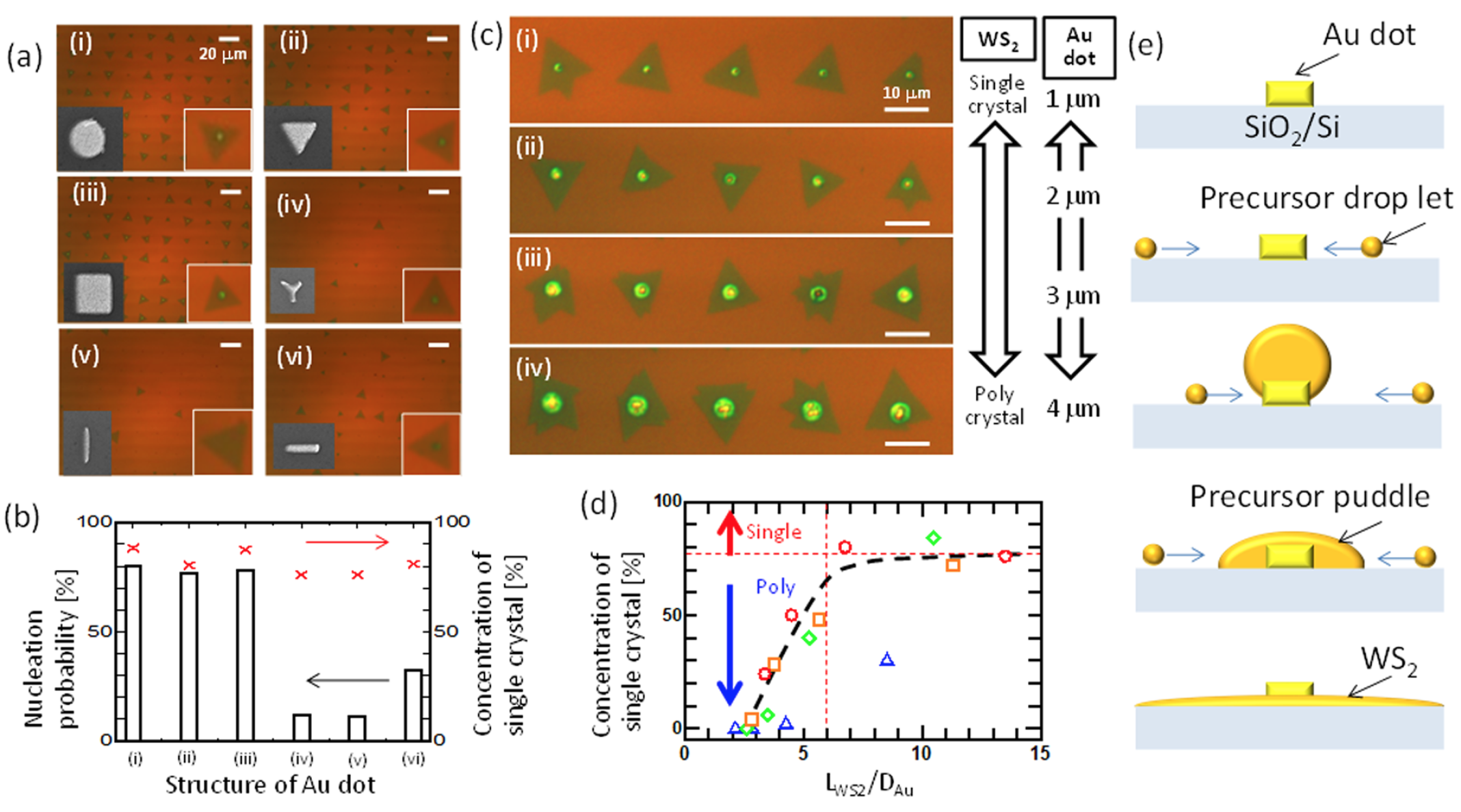
Image No. 3
To better understand the dynamics of WS 2 formation, experiments were conducted in which the shape and diameter of gold inclusions (D Au ) were varied ( 3a ). A strong correlation was observed between the structure of the nucleation point and the probability of nucleation of WS 2 ( 3a and 3b ).
It was also noted that the crystallinity of the WS 2 monolayer was in no way dependent on the shape of the gold inclusions; the WS 2 single crystals grew equally well in round, triangular, square, and rod-shaped areas.
Further, scientists concentrated their shooting precisely on round disseminations of gold, changing their diameter, and the influence of different temperatures was also monitored. The experiment revealed that at D Au ~ 1 μm, the concentration of the single crystal WS 2 was higher than at D Au ≈ 4 μm, i.e. the concentration was higher with growth on smaller inclusions of gold ( 3s ).
Changing the growth temperature allowed us to change the value of L WS 2 . The plot of the dependence of the single crystal concentration on L WS 2 / D Au showed a clear correlation: the concentration of WS 2 single crystals increased with LWS 2 / D Au and reached saturation at (L WS 2 / D Au )> 6 ( 3d ).
Summarizing the observational data as follows:
the diffusion length of the precursor was superlong (~ 750 μm);
single crystals can grow on interspersed gold (Au) of various shapes;
there is a clear correlation between the concentration of the single crystal and L WS 2 / D Au .
Based on the data obtained from observations, scientists proposed their model of diffusion and nucleation of the precursor ( 3e ). Since the shape of the gold inclusions is in no way related to the growth of WS 2 , it is worth suggesting that a round “puddle” (in the 3rd puddle ) of the precursor could form around the interspersed Au even before the two-dimensional growth. In addition, the growth of polycrystalline WS 2 will be possible if the diameter of the precursor puddle will be smaller than the diameter of the inclusions of gold (D Au ). Consequently, the precursor will diffuse onto the substrate in the form of droplets, and not in the form of individual molecules, which explains the extra long diffusion of the precursors on the SiO 2 substrate.
In addition, the interaction between the droplets and the substrate occurs through physical adsorption, rather than chemical. And this is completely different from atomic and molecular diffusion, where the NN jump is dominant due to strong chemical interactions with the surface of the substrate. Physically adsorbed droplets easily move along the surface of SiO 2 for a relatively long time, which ensures ultra-long diffusion.
The scientists determined the stability of the droplets using the Young-Laplace equation: ΔP = 2γ / r, where ΔP is the difference between the drop pressure (P in ) and the vapor pressure (P out ) at the interface; γ is the surface tension of the droplet; r is the radius of the drop.
The smaller the ΔP value, the more stable the drop will be. This means that materials with low γ are more stable, especially in the nanoscale range (r <500 nm). The value of γ drops of molten metals can be reduced by increasing the temperature, reducing the size of the droplets and mixing them with oxygen. It can be assumed that nanoscale droplets containing WxSyOz at high temperatures will exhibit very low surface tension, making them candidates for precursor droplets. Researchers note that in order to better understand WS 2 growth dynamics, it is necessary to carefully study the components of precursor droplets.
All calculations, theories, and experimental results can be confirmed by a very simple, but at the same time complicated way, by direct observation of the nucleation phase.
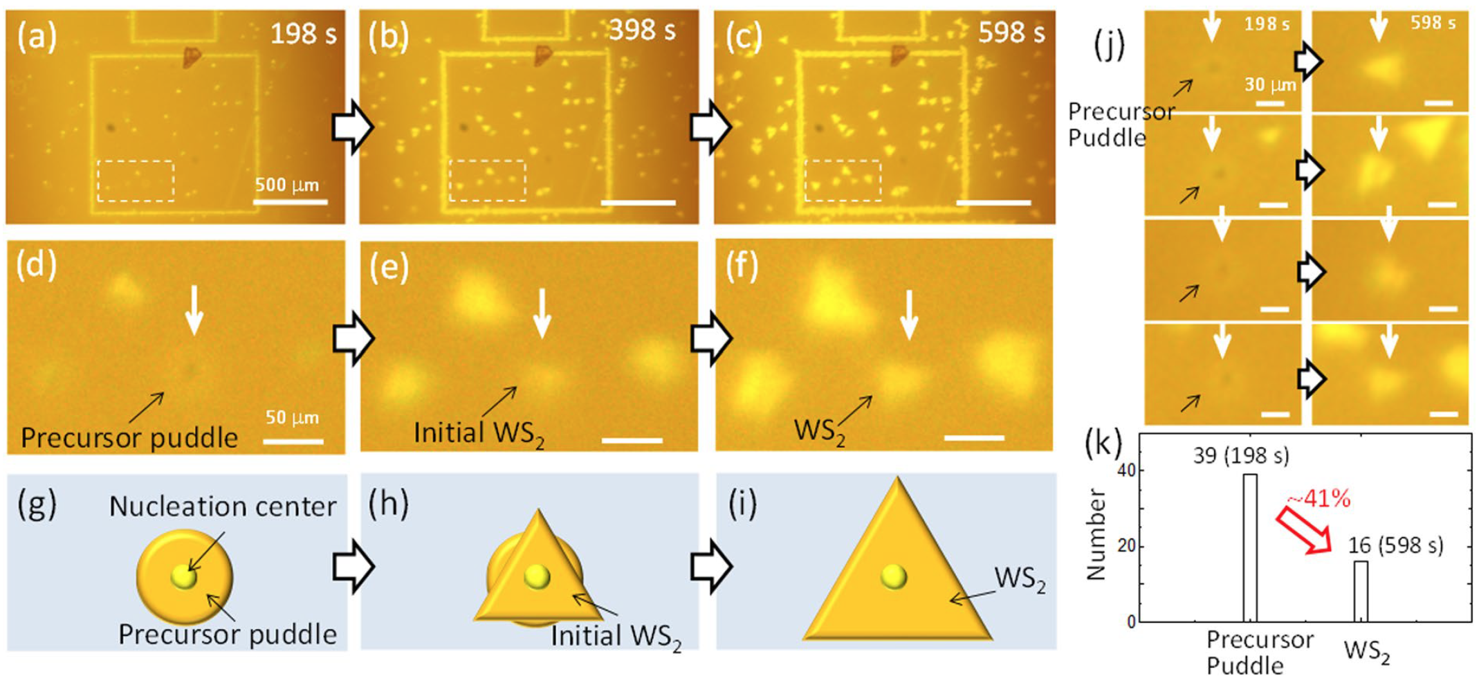
Image No. 4
During direct observation (in real time), an increase in LWS 2 was observed, which confirms the very possibility of real-time observation of WS 2 crystal growth ( 4a - 4c ).
A detailed study of nucleation allowed us to see an interesting transformation ( 4d - 4f ). At the beginning of growth, ring structures ( 4d and 4g ) formed around the natural center of nucleation. They changed to triangular shapes at the growth stage ( 4e , 4f , 4h and 4i ). These observations are consistent with the model described previously ( 3e ). Therefore, this indicates a pool of precursor formed immediately after nucleation around its center. Similar transformations from pools of precursors in WS 2 were observed in many nucleation sites ( 4j ), which established the reliability of the growth dynamics caused by drops ( 3e and 4g - 4i ).
It was found that about 41% of the precursors are converted to WS 2 during the growth stage.
The main fact that confirms the presence of several growth mechanisms of PDMs at once is the formation of a part of WS 2 crystals even without pools of precursors.
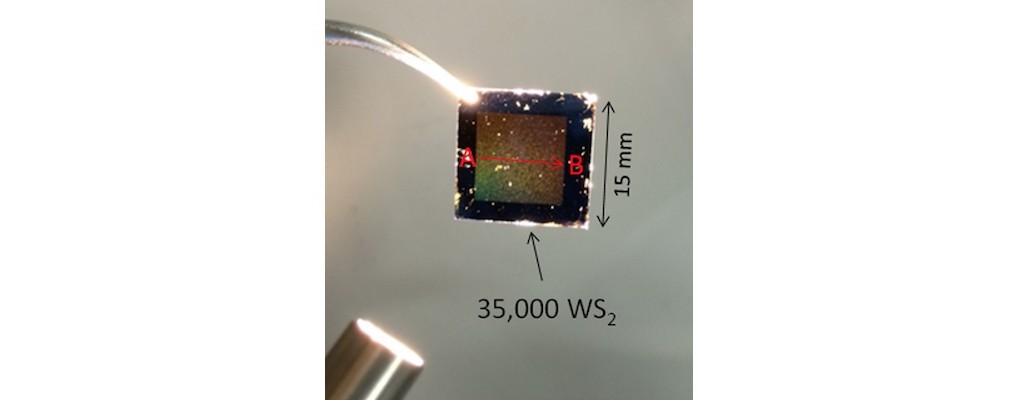
Further, based on the studied growth model, the scientists made precise adjustments to D Au , L Au and growth temperature in a combinatorial experiment. These systematic adjustments created the conditions necessary for the integrated synthesis of WS 2 single crystals, which was determined by the balance between the probability of nucleation and the growth of a single crystal. Under the most suitable growth conditions, integrated WS 2 was grown in the region of 1.5 cm x 1.5 cm, which covered the entire substrate ( 5a ).
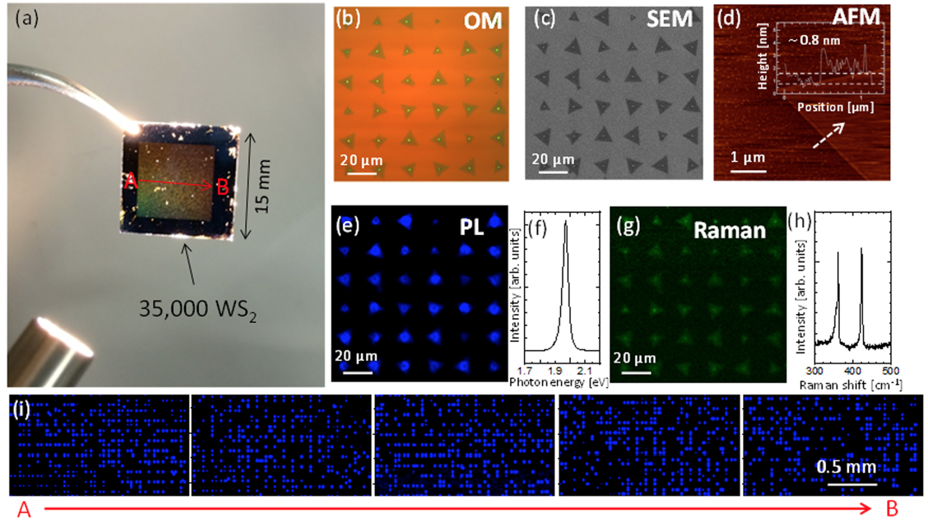
Image No. 5
Images obtained using an optical microscope ( 5b ) and scanning electron microscope ( 5c ) showed that triangular WS 2 crystals grew on Au points with a result of> 87%. Atomic force microscopy showed that the thickness of WS 2 was approximately 0.8 nm ( 5d ). Crystalline WS 2 shown on the photoluminescence intensity map ( 5e ) showed bright photoluminescence with a sharp emission peak at 1.97 eV ( 5f ).
The Raman spectra of WS 2 contained two peaks separated by 61 cm −1 ( 5g and 5h ). This suggests that WS 2 grown by this method is a monolayer single-crystal structure.
Mapping of the PL intensity was carried out over a large area between A and B ( 5a ). Uniform photoluminescence was detected over the entire width (1.5 cm) of the substrate ( 5i ).
All these observations have confirmed that> 35,000 individual WS 2 crystals can be grown with precise position control.
For a more detailed acquaintance with the nuances of the study, I recommend that you look into the report of scientists and additional materials to it.
Epilogue
In this work, scientists were able to demonstrate the results of the world's first direct real-time observation of the growth of WS 2 crystals. This allowed a much better understanding of the growth dynamics of the monolayer and single crystal WS 2 . By controlling the nucleation due to Au points and diffusion barriers, a record value of the diffusion length L d ~ 750 μm was achieved, which is almost two orders of magnitude greater than that of traditional semiconductor materials.
By putting together all their theories, calculations and observations, scientists were able to implement a combinatorial experiment, the result of which was the successful growth of more than 35,000 WS 2 single crystals on a substrate with a width of only 1.5 cm.
The researchers themselves believe that the results of their work will serve as the basis for a successful transition from studying the fundamental principles of the formation of transition metal dichalcogenides to practical experiences and the implementation of knowledge gained in the process.
By fully understanding the nature, properties and characteristics of such unusual compounds as transition metal dichalcogenides, new types of semiconductors will be created, the thickness of which will be only a few atoms, and the efficiency will not be inferior to classical semiconductors. Such developments will be extremely useful in all types of electronics, especially in flexible ones.
Do we all know about transition metal dichalcogenides? Of course, far from all. However, thanks to this kind of research, the spectrum of our knowledge is expanding, which in the future will allow us to completely change our understanding of not only semiconductors, but also the world around us.
Thank you for your attention, remain curious and have a good working week, guys! :)
Thank you for staying with us. Do you like our articles? Want to see more interesting materials? Support us by placing an order or recommending it to your friends, a 30% discount for Habr users on a unique analog of entry-level servers that we invented for you: The whole truth about VPS (KVM) E5-2650 v4 (6 Cores) 10GB DDR4 240GB SSD 1Gbps from $ 20 or how to divide the server? (options are available with RAID1 and RAID10, up to 24 cores and up to 40GB DDR4).
Dell R730xd 2 times cheaper? Only we have 2 x Intel TetraDeca-Core Xeon 2x E5-2697v3 2.6GHz 14C 64GB DDR4 4x960GB SSD 1Gbps 100 TV from $ 199 in the Netherlands! Dell R420 - 2x E5-2430 2.2Ghz 6C 128GB DDR3 2x960GB SSD 1Gbps 100TB - from $ 99! Read about How to Build Infrastructure Bldg. class c using Dell R730xd E5-2650 v4 servers costing 9,000 euros for a penny?
All Articles