Development of HDMI fiber optic extension cable for 300 meters. Refusal of the return channel (data transmission on one fiber-optic cable). Cloning EDID from the monitor.
The HDMI standard is widely used in many areas where image output to the screen is required. Personally, I was able to transmit the signal via an HDMI cable to a distance of 10 meters (it was simply not required anymore). I think that without loss of quality, you can transfer the picture to a distance of 30-40m. The main disadvantages in the case of broaching such a cable are its diameter and size, directly, of the connectors. The easiest way to exclude the cable is to use a wireless extension cord, I think it will be possible to reach 100-150 meters, but I will not say for sure. Unfortunately, not all objects, for one reason or another, allow the use of wireless networks. And if you need even further?
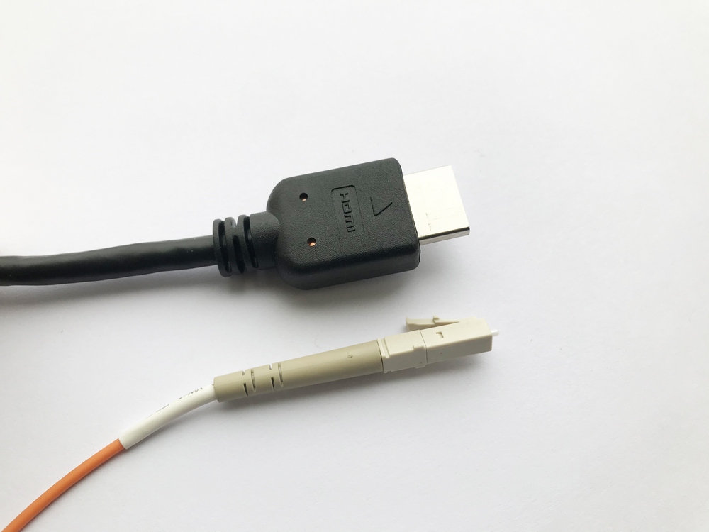
Fig. 1. HDMI cable and optics (LC)
Of course, optics is probably not the best option for transmitting video, but when using stationary PCs and monitors, it’s even nothing. The first thesis is the diameter of the optical cable (in my case, it is 2-3mm) and the diameter of the connector of the fiber optic cable. The second is, of course, the distance. Looking ahead, I will say that the tests were carried out on a 300m cable, diameter (external) - 3mm.
Elemental base
When working out the element base, the choice, unexpectedly, fell on the Chinese company SiFotonics, which specializes in this kind of equipment. To begin with, we studied their products and got two debugs that we connected with a three-hundred-meter optical cable and made sure that everything worked flawlessly. They also have SFP optical receivers / transmitters (ROSA / TOSA), serializers / deserializers, drivers, etc.
Principle of operation
To connect and operate the devices, you need to connect two optical cables and apply power (microUSB cable). If we give an analogy with a conventional HDMI cable, in which there is I2C for exchanging an EDID table, then everything is the same - one channel for data transfer, the second - for transferring EDID from the monitor to the video card. Data is transmitted at a speed of 10Gbps. Tearing off the cable of the return channel, the picture invariably disappears. At this point, some doubts crept in, and whether any service data or synchronization marks are being transmitted in the return channel, or maybe the devices are monitoring connections to each other ...

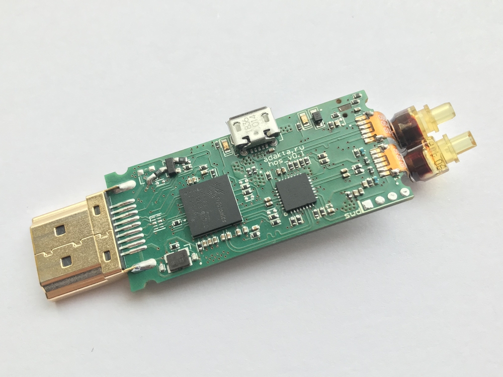
Fig. 2. The composition of the modules
The first iteration of the board, it is also a layout, turned out to be 20X45mm in size. With a “side” power connector, to make it easier to distribute power buses in landfills. Total 4 layers turned out. Why this PCB configuration is bad, I will write later. Tricky debugging developers used 0201 passive, which I absolutely didn’t want to do, so I used 0402 and a capacitor porridge under the chip.
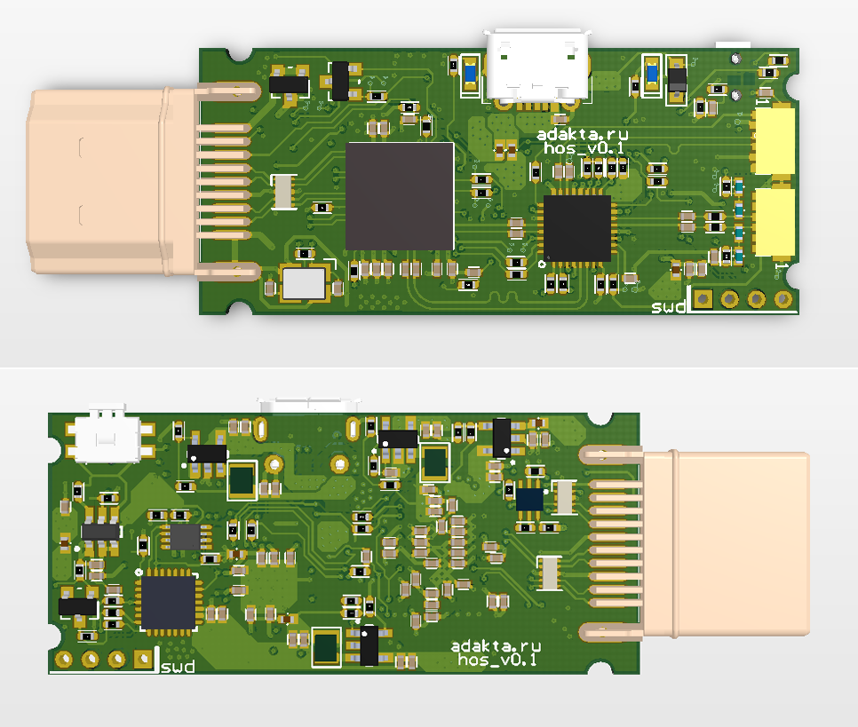
Fig. 3. 3D model of the source module board layout
As I wrote above, my task was not only to make a couple with a working distance of 300 meters, but also to remove the return channel of the optics. At the design stage, we decided not to get involved in finalizing the Chinese software (although we were kindly provided with all the sources), because, firstly, this is a bunch of incomprehensible code lines in an incomprehensible compiler, and secondly, SiFotonics can supply flashed chips, which It’s very convenient, since it’s very difficult to flash devices as part of production. So that the reader does not think that I am exaggerating when speaking about the difficulties, I will give a photo of the programming stand.
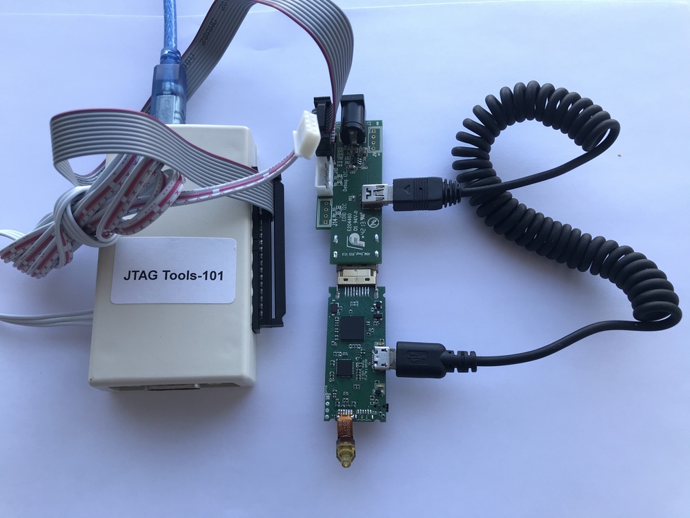
Fig. 4. Stand for programming and diagnostics
Yes, yes, as you probably already guessed, the JTAG contacts for programming are output to microUSB contacts, and to some HDMI contacts that used to be GND. Immediately make a reservation that this did not affect the quality of work. So, stand. To program the chip, you must first collect one circuit diagram of the stand and put the chip in programming mode using specialized software. Next, you need to assemble another circuit and use the other software to flash the board. After that, it automatically goes into working mode.
In general, it seems to me that this is impractical even for 1000 pieces.
Let's go back to the reverse channel. To store EDID tables, we need an EEPROM, and we will need to change its address on the fly. He took the N24C02UDTG in a miniature US-8 package. For its programming, I use the STM32F031G4U6 microcontroller, also in the smallest package that can be found in the public domain - UFQFPN-28. I also took the TPS27081ADDCR power switch. And here is what I got:
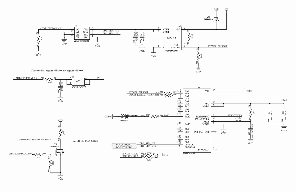
Fig. 5. EDID cloning implementation scheme
The idea is as follows. This circuit is implemented on the transmitting module (the one that connects to the PC). To clone an EDID monitor, the device connects to the monitor. By default, the EEPROM address on our module should not coincide with the EEPROM address in the monitor (while reading), that is, it can be any other, for example, I made the A0 leg manageable. At the time of connecting to the monitor, power is supplied to the EEPROM, and leg A0 is pulled up to the logical "0" resistor. Two EEPROMs with the same addresses are hanging on the i2c bus, but this is not critical, since we are not working with them yet. In my circuit there is also a button and LED for indicating power / firmware EDID / errors. A short press of the button changes the address and allows the microcontroller to start reading / writing EDID. We reset the EEPROM with power (just in case) when we received the signal from the button, read the EDID of the monitor and immediately write it to our chip. We blink 3 times with the LED and turn off the power of the EEPROM. Reading / writing occurs instantly, so a forced delay is made for blinking, so that the user understands that something is happening. That is, we begin to blink when it is already possible to let go. If something is wrong, then do not light the LED.
Next, connect the module to the PC and immediately see the new monitor in the settings. The problem is solved.
For programming the microcontroller brought the SWD bus.

Fig. 6. Reverse side of the module board
Features
After all the work done with EDID cloning, I removed the reverse optical channel and everything worked flawlessly. In these experiments, the power came from a USB PC. At boot time, the computer (in any case mine) turns off the USB power for a moment and the BIOS picture blinks on the monitor - this is not critical. Then I dropped out the reverse channel modules from the devices and after this blinking the picture stopped recovering. And this happened precisely because of the lack of a TOSA module on the monitor device. I tried to emulate the presence of a laser, but all to no avail. I am almost sure that this problem can be solved by firmware, but we decided not to get into it. A miracle happened when I connected both devices (receiver and transmitter) to power supplies (as, by the way, it was indicated in the statement of work). The picture stopped blinking, and accordingly disappear. If you distort the power of the devices during operation, the picture is restored without problems.
Fig. 7. Transmitter (laser) switching circuit
Now back to the PCB configuration and the side power connector. This implementation was initially inconvenient and suitable only for the layout. In the release device, I reduced the width of the board to 16.3 mm and put the power connector in place of the optical module of the reverse channel - this will allow you to include several devices in one video card. Otherwise, the power connector interfered with me and the board was very wide.
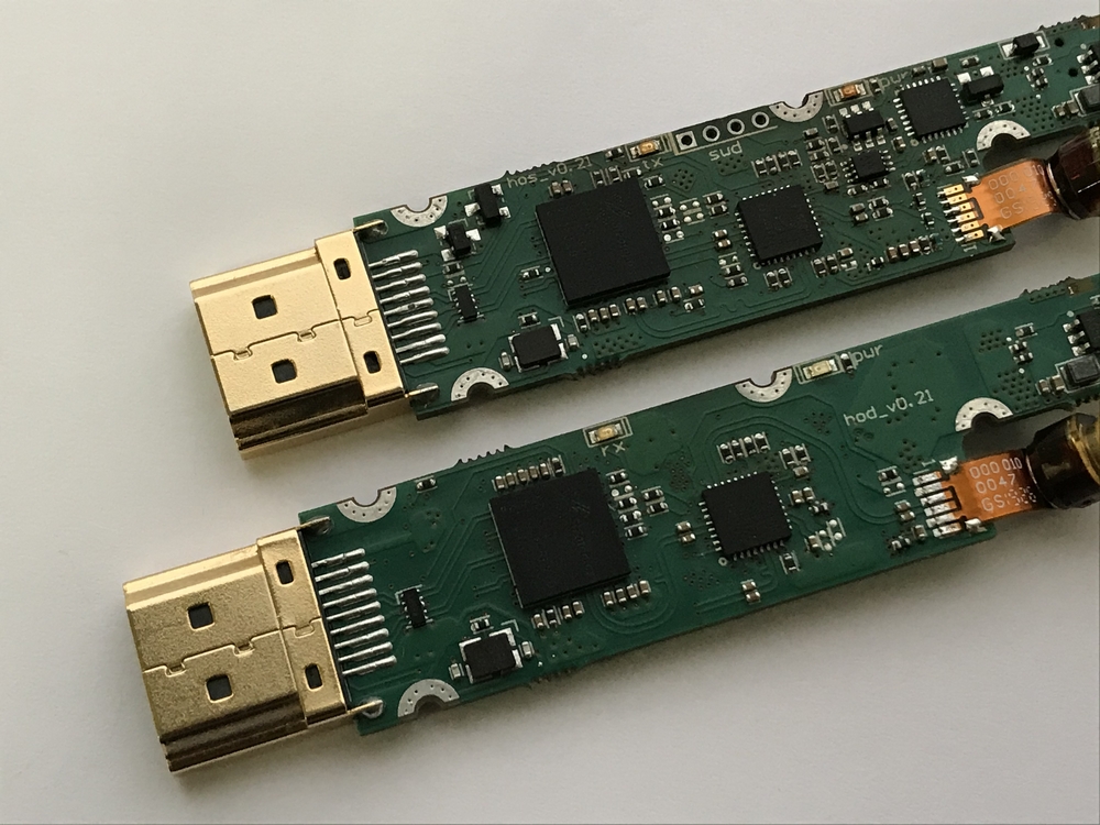
Fig. 8. Narrow receiver and transmitter boards
Here, of course, there were many re-wiring and rearrangements of components. The supply ranges were completely redone to optimize for these sizes and transfer the microUSB connector. As you can guess, the cases for both devices are identical, therefore the board configuration, connectors and optical module are located the same. The body is milled from aluminum and is a heat sink for the processor and driver. The protrusions for these components are milled on the inside, so they are also located the same way.
Conclusion
At the moment, four pairs of devices are soldered, tests are carried out on a long cable on different monitors and TV. There are no complaints about the work. We check only on fullHD and below.
Thank you and see you soon!