Destroy America's monopoly in the EDA. Innopolis takes the first step
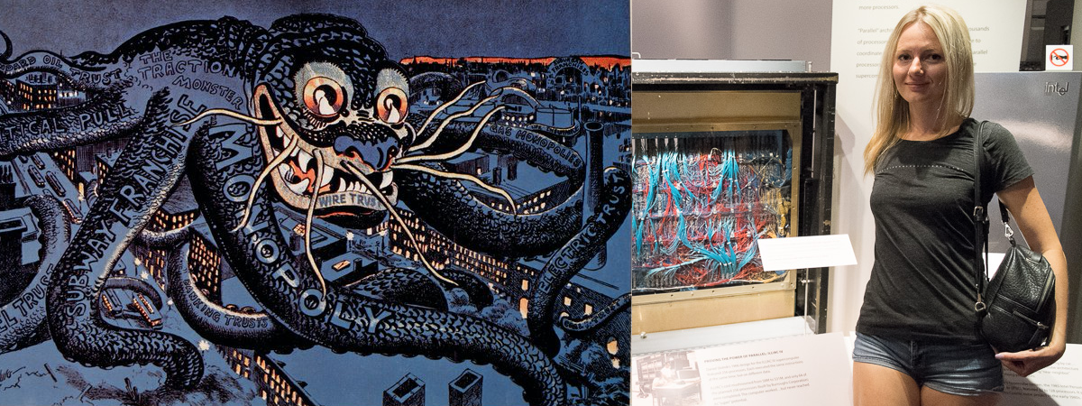
Since the 1990s, it has amazed me that the design of the entire world of digital microelectronics is controlled by two offices in California, which are 10 minutes from each other - Synopsys and Cadence. At that time, a quarter of the world's design was done in Japan (mainland China was then in a primitive state), and all these Sony, Hitachi, Fujitsu and other giants bowed to America and paid uncountable millions of dollars for the programs that Japanese designers then used. Now it continues with Samsung, Huawei and even with Russian offices that design microchips for space.
The Russian land managed to grow Yandex versus Google, so why not try to create some programs for designing microchips? You can start small: to popularize competitions and hackathons for the development of design automation algorithms (Electronic Design Automation - EDA). These algorithms are convenient in that they have many levels of complexity: a student can write the simplest Place & Route program over the weekend, but an advanced program will require decades of work for hundreds of people and billions of dollars in R&D.
Now in Innopolis near Kazan they are doing an event for students in the format of "two weeks of training + hackathon . " One of the topics was the traditional task of EDA - placing and tracing a graph of an electronic circuit into rows of standard cells. It will be interesting to see what a small team of programmers with a basic understanding of C ++ / Java / Python, methods for parsing text, graph algorithms and skills to visualize data structures using the GUI can implement in a short time.
So - the statement of the problem:
The task consists of three subtasks that different students can deal with:
- Parsing the text representation of a digital circuit graph.
- Placing a graph on the rows of standard cells of the microcircuit and connecting these cells with tracks (tracing).
- Visualization of the results - display on the screen of the circuit tracks and connections.
The input to the program is a text file in a very limited subset of the Verilog hardware description language. This file describes the inputs and outputs for the circuit (input, output), internal connections (wire) and provides a list of logic elements in the format "instance-name type (list of connections)". The file can be parsed in C / C ++ using Lex + Yacc or similar programs.

The result of parsing the text should be a representation of the graph of the elements in memory. This view will be used by the placement and tracing algorithm, which will then be created by another structure. If there are enough participants in the hackathon team, the result of the initial parsing can be visualized during the hackathon as an additional task. Approximately in this spirit, even if not so beautiful:

If there are not enough participants during the hackathon, then the visualization of the intermediate, unplaced graph should be left for later, and during the hackathon, only the final placement should be displayed on the screen.
In general, the parsing task can be posed with several levels of complexity:
- In the simplest cases, all nodes of the graph are two-input logical elements AND and OR, as well as single-input NOT elements. At the final placement, they are implemented by standard cells of the same width.
- If there is enough time for the hackathon, the task can be complicated:
- introduce three- and four-input cells AND3, OR4, etc .;
- expand the set of node types by adding NAND, XOR, D-flip-flops (D-Flip-Flop) with different options (reset, enable), etc .;
- make an additional text file in which to set the width and other parameters of the cells.
- After the hackathon, the task can be tied to the real world, and it is parsing not abstract AND and OR, but a file in the same format, but with cells from real libraries of standard ASIC cells at 28, 14 or 7 nanometers, which are supplied to EDA developers and factory designers type TSMC (Taiwan Semiconductor Manufacturing Company).
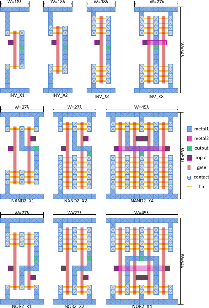
What is a standard cell? This is a standard height cell for this ASIC library, that is, a library of primitives for manufacturing a microcircuit in a factory using some technology. ASIC - Application Specific Integrated Circuit. Now most chips, such as smartphones, are ASICs. The cells in the ASIC library have a standard height so that they can be conveniently arranged in rows to supply power to them and facilitate trace algorithms. Different cells in the library can implement not only primitives such as AND and OR, but also more complex constructions - multiplexers, latches, combinations of two or three logic elements (AND-OR), etc.
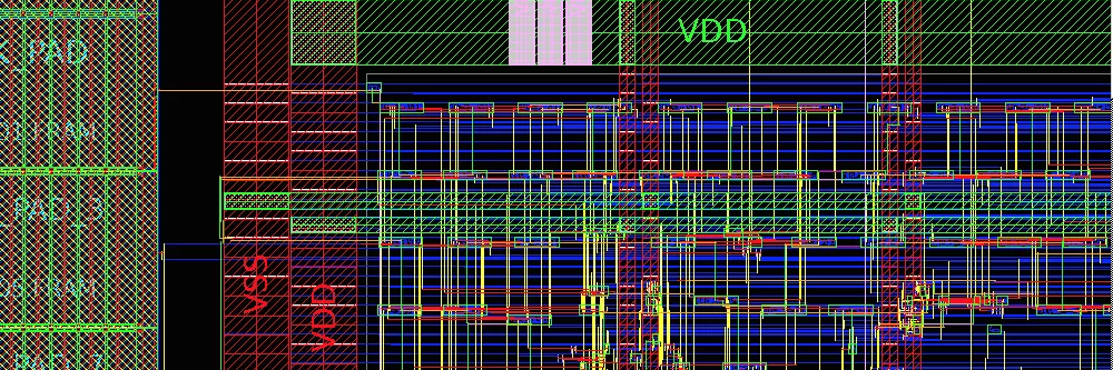
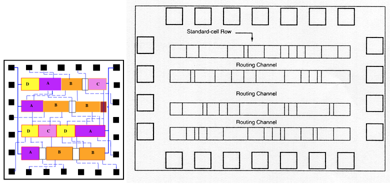
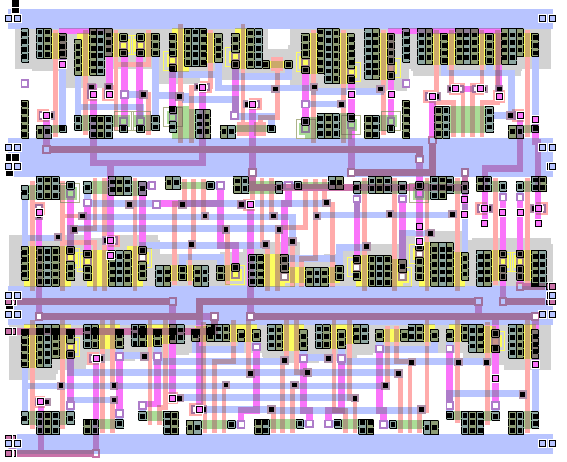
Cells on the microcircuit line up in rows (slide from Charles Danchek 's lectures ):

Between rows there are channels (routing channels) in which connections pass. The width of the channels can be changed if congestion is formed in the connections. In the rows, you can make gaps between the cells:
For a hackathon, the task can be simplified to the level of a spherical horse in a vacuum:
- Limit cell types. For starters, you can generally place just a graph of two-input NAND.
- Consider all cells to have the same width.
- Ignore all aspects of the physical nature of cells, including signal delay and power consumption.
Here, “ignore” means that in the training exercise you can not take cell physics into account when assessing the quality of placement and tracing. To begin with, it is enough to consider only the geometry, for example, to minimize the total length of the joints and the number of layers on which the joints are made. The need for a new layer arises when it is impossible to place two conductors without crossing them.
At the hackathon, it is enough to consider standard cells as “black boxes” and display them on the screen as in the figures above. Or with images of logical elements, as on a slide from Igor Markov's lectures :

Although if you display with the insides of the cells, then the pictures are more decorative. A slide from the lectures of Charles Danchek :

Another picture from the Internet with the placement and tracing + image of the insides of the cells:
But how to place cells in rows, expand and narrow channels between rows, build connections, introduce new layers, evaluate the optimality of results and sort through options? Well, these are purely algorithmic and programming tasks, in Innopolis they probably teach this, therefore I will not spread my thoughts or thoughts on the tree. As an initial inspiration for tracing, you can use the ancient method of wave tracing, which is described in the third part of the course for schoolchildren from RUSNANO . Although this method is not for standard cells arranged in rows, but for a less ordered case with a small number of components:
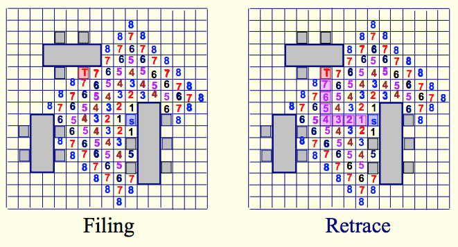
2.10. How to do it: Wave tracing algorithm.
One of the classic algorithms used by early tracing programs was wave tracing, which was described in a 1961 article by Chester Lee, a researcher at Bell Labs. In English, the Lee algorithm is called “maze routing,” which literally translates as “labyrinth tracing.” This name is due to the fact that in addition to programs for designing electronics, the Lee algorithm was used in game programs to find the shortest path in the maze.
The Lee algorithm represents the blocks that need to be connected, in the form of figures on a limited plane, marked "in the box". To find the shortest path from the output of one block to the output of another block, the Lee algorithm uses two passes:
- The first pass is called wave propagation. We mark all “cells” or a cell at the first output with a unit. After that, for each cell labeled with the number N, we mark all the neighboring free unlabeled cells with the number N + 1. Repeat the markup until we either reach the conclusion of the second block or there is no more opportunity to spread the “wave”.
- The second passage is called "restoration of the path." If the cell at the second block is marked, we will choose among its neighbors a cell that is marked 1 less than the number in the current cell. Add a neighboring cell to the path, go into it and begin to look at its neighbors, which are marked 1 less. We repeat this until we come to the conclusion of the first block.
First, the Lee algorithm was used in programs for the design of printed circuit boards, then they began to use it for the design of microcircuits. However, when the size of the microcircuits grew, it was impossible to apply the Lee algorithm in its original form, since it requires a large amount of memory to store the data array, as well as a large amount of time for numerous passes through this array. Despite the fact that modern automatic tracing programs use other algorithms, the Lee algorithm remains an excellent exercise for those who have recently mastered programming and want to write a small tracing program themselves.

For more serious algorithms, you can search for ideas in the materials of Igor Markov . But the best thing would be to be creative - what if you come up with something that thousands of mathematically-savvy algorithmic programmers haven’t come up with traffic jams on the 101st, 880th and 237th freeways in Synopsys and Cadence offices every morning in the cities of San Jose, Sunnyvale and Mountain View, California.
References (from simple to complex):
- Introductory lectures on the basics of digital design in Innopolis: 1 , 2 .
- Introductory course in digital electronics and EDA for advanced schoolchildren of the olympiad type. From RUSNANO: 1 , 2 , 3 .
- Textbook Harris & Harris .
- Slides of lectures by Charles Danchek .
- Course by Igor Markov from the University of Michigan . He read this course at Moscow State University.
I hope that the initiative of Innopolis in algorithmic competitions will expand. The EDA area is mathematically interesting and well paid. Synopsys opened a branch in Armenia and turned into one of the leading employers there: “Today, Synopsys is one of the largest IT employers in Armenia with more than 650 employees (including more than 600 engineers).” I note that Russia is larger than Armenia and probably can create your own synopsys. In the end, there are many programmers in Russia, mathematicians too, and the current market capitalization of Synopsys + Cadence is approximately equal to the costs of the Sochi Olympics.
All Articles