The future of Li-Fi: polaritons, excitons, photons and some tungsten disulfide

For many years, scientists from around the world have been doing two things - inventing and improving. And sometimes it’s not clear which of this is more difficult. Take, for example, ordinary LEDs that seem so simple and ordinary to us that we do not pay attention to them. But if you add a little excitons to them, a pinch of polaritons and tungsten disulfide to taste, the LEDs will no longer be so prosaic. All these abstruse terms are the names of extremely unusual components, the combination of which allowed scientists from New York City College to create a new system that can transmit information extremely quickly with the help of light. This development will help improve the technology of Li-Fi. What exactly were the ingredients of the new technology used, what is the recipe for this “dish” and what is the efficiency of the new exciton-polariton LED? This will tell us the report of scientists. Go.
Study basis
If everything is simplified to one word, then this technology is light and everything connected with it. Firstly, polaritons that arise when photons interact with excitations of the medium (phonons, excitons, plasmons, magnons, etc.). Secondly, excitons are electronic excitation in a dielectric, semiconductor, or metal, migrating through a crystal and not related to the transfer of electric charge and mass.
It is important to note that these quasiparticles are very fond of cold, i.e. their activity can be observed only at extremely low temperatures, which greatly limits practical application. But that was before. In this work, scientists were able to overcome the temperature limit and use them at room temperatures.
The main feature of polaritons is the ability to bind photons to each other. Photons colliding with rubidium atoms gain mass. In the process of multiple collisions, photons bounce from each other, but in rare cases form pairs and triplets, while losing the atomic component represented by the rubidium atom.
But in order to do something with the light, it must be caught. For this, we need an optical resonator, which is a set of reflective elements that form a standing light wave.
In this study, the most important role is played by even more unusual quasiparticles — exciton polaritons, which are formed due to the strong coupling of excitons and photons trapped in the optical resonator.
However, this is not enough, for a material basis is needed, so to speak. And who better than others will play this role if not transitional metal dichalcogenide (PDM). More precisely, the monolayer WS 2 (tungsten disulfide), which has impressive exciton binding energies, was used as the emitting material, which became one of the main criteria for choosing the material basis.
The combination of all the above elements made it possible to create an electrically controlled polariton LED operating at room temperature.
To implement this device, the WS 2 monolayer is located between thin hexagonal boron nitride (hBN) tunnel barriers with graphene layers acting as electrodes.
Research results
WS 2 , being a transition metal dichalcogenide, is also an atomically thin Van der Waals (vdW) material. This indicates its unique electrical, optical, mechanical and thermal properties.
In combination with other vdW materials, such as graphene (as a conductor) and hexagonal boron nitride (hBN, as an insulator), a whole host of electrically controlled semiconductor devices can be realized, which include LEDs. Similar combinations of Van der Waals materials and polaritons have already been implemented previously, as the researchers openly state. However, in previous works, the resulting systems were complex and imperfect, and also did not reveal the full potential of each of the components.
One of the ideas inspired by the predecessors was the use of a two-dimensional material platform. In this case, it is possible to implement devices with atomically thin emission layers, which can be integrated with other vdW materials acting as contacts (graphene) and tunnel barriers (hBN). In addition, such two-dimensionality makes it possible to combine polariton LEDs with vdW materials with unusual magnetic properties, strong superconductivity, and / or non-standard topological transfers. As a result of this combination, you can get a completely new type of device, the properties of which can be very unusual. But, as scientists say, this is a topic for another study.
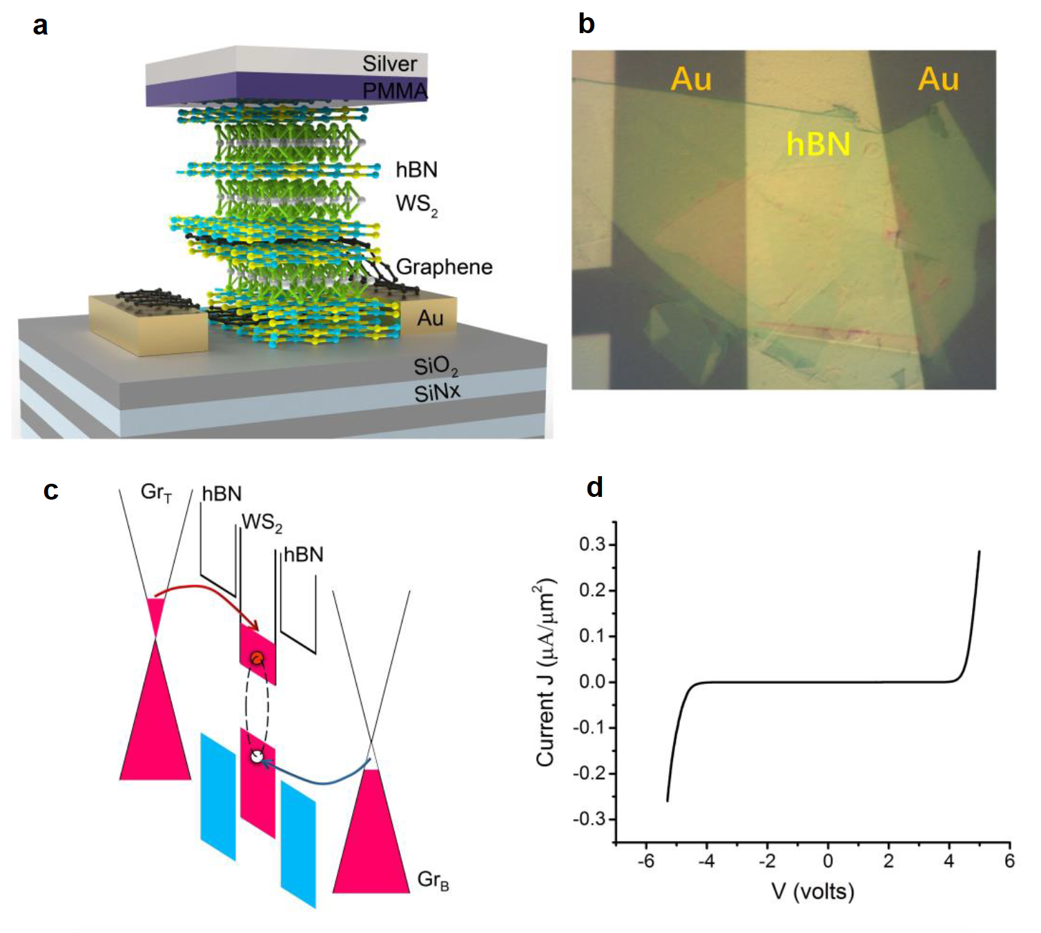
Image No. 1
Image 1a shows a three-dimensional model of a device that resembles a layer cake. A silver layer acts as the upper mirror of the optical resonator, and a 12-layer distributed Bragg reflector * acts as the lower one. In the active region there is a tunnel zone.
Distributed Bragg reflector * - a structure of several layers, in which the refractive index of the material periodically changes perpendicular to the layers.The tunnel zone consists of a vdW heterostructure consisting of a monolayer WS 2 (light emitter), thin hBN layers on both sides of the monolayer (tunnel barrier) and graphene (transparent electrodes for the introduction of electrons and holes).
Two more WS 2 layers were added to increase the total generator strength and, therefore, for a more pronounced Rabi splitting of polariton states.
The resonator operating mode is adjusted by changing the thickness of the PMMA layer (polymethylmethacrylate, i.e., plexiglass).
Image 1b is a snapshot of the vdW heterostructure on the surface of a distributed Bragg reflector. Due to the high reflectivity of the distributed Bragg reflector, which is the lower layer, the tunnel zone in the image has a very low reflection contrast, as a result of which only the upper thick hBN layer is observed.
Graph 1c is a zone diagram of the vdW heterostructure in the tunnel geometry at offset. Electroluminescence (EL) is observed above the threshold voltage when the Fermi level of the upper (lower) graphene is shifted above (below) the conduction (valency) band of WS 2 , allowing the electron (hole) to tunnel into the conduction (valency) band of WS 2 . This creates favorable conditions for the formation of excitons in the WS 2 layer with subsequent radiation (radiative) electron – hole recombination.
Unlike light emitters based on pn junctions, which require doping, the EL from tunneling devices depends exclusively on the tunneling current, which avoids optical losses and any changes in resistivity caused by changes in temperature. At the same time, the tunnel architecture allows a much larger radiation area compared to pn junction based dichalcogenide devices.
Figure 1d shows the electrical characteristics of tunnel current density ( J ) as a function of bias voltage ( V ) between graphene electrodes. A sharp increase in current for both positive and negative voltage indicates the appearance of a tunneling current through the structure. At the optimal layer thickness hBN (~ 2 nm), a significant tunneling current and an increase in the lifetime of the introduced carriers for radiative recombination are observed.
Before the electroluminescent experiment, the device was characterized by the reflectivity of white light with angular resolution to confirm the presence of a strong exciton coupling.
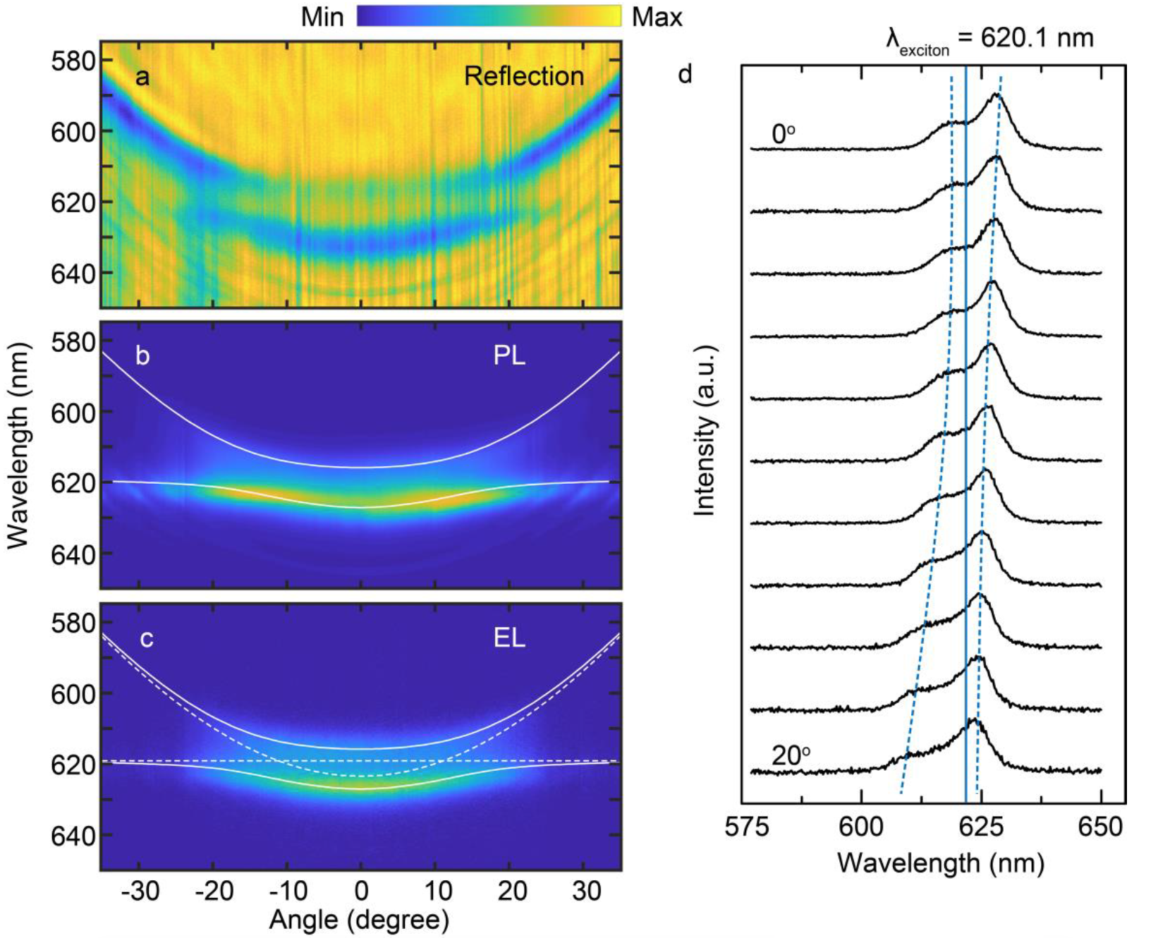
Image No. 2
Image 2a shows reflection spectra with a resolution in the angle from the active region of the device, showing the behavior that prevents the intersection. Photoluminescence (PL) was also observed under nonresonant excitation (460 nm), which showed intense radiation from the lower branch of the polariton and weaker radiation from the upper branch of the polariton ( 2b ).
2c shows the dispersion of the electroluminescence of polariton with the introduction of 0.1 μA / μm 2 . The Rabi splitting and resonator detuning obtained by fitting the oscillator modes (solid and dashed white lines) to the electroluminescent experiment are ~ 33 meV and ~ -13 meV, respectively. The resonator detuning is defined as δ = E c - E x , where E x is the exciton energy, and E c denotes the photon energy of the resonator with zero momentum in the plane. Graph 2d is a slice at different angles from the electroluminescent dispersion. Here, the dispersion of the upper and lower polariton modes with anti-intersection occurring in the exciton resonance zone is clearly visible.
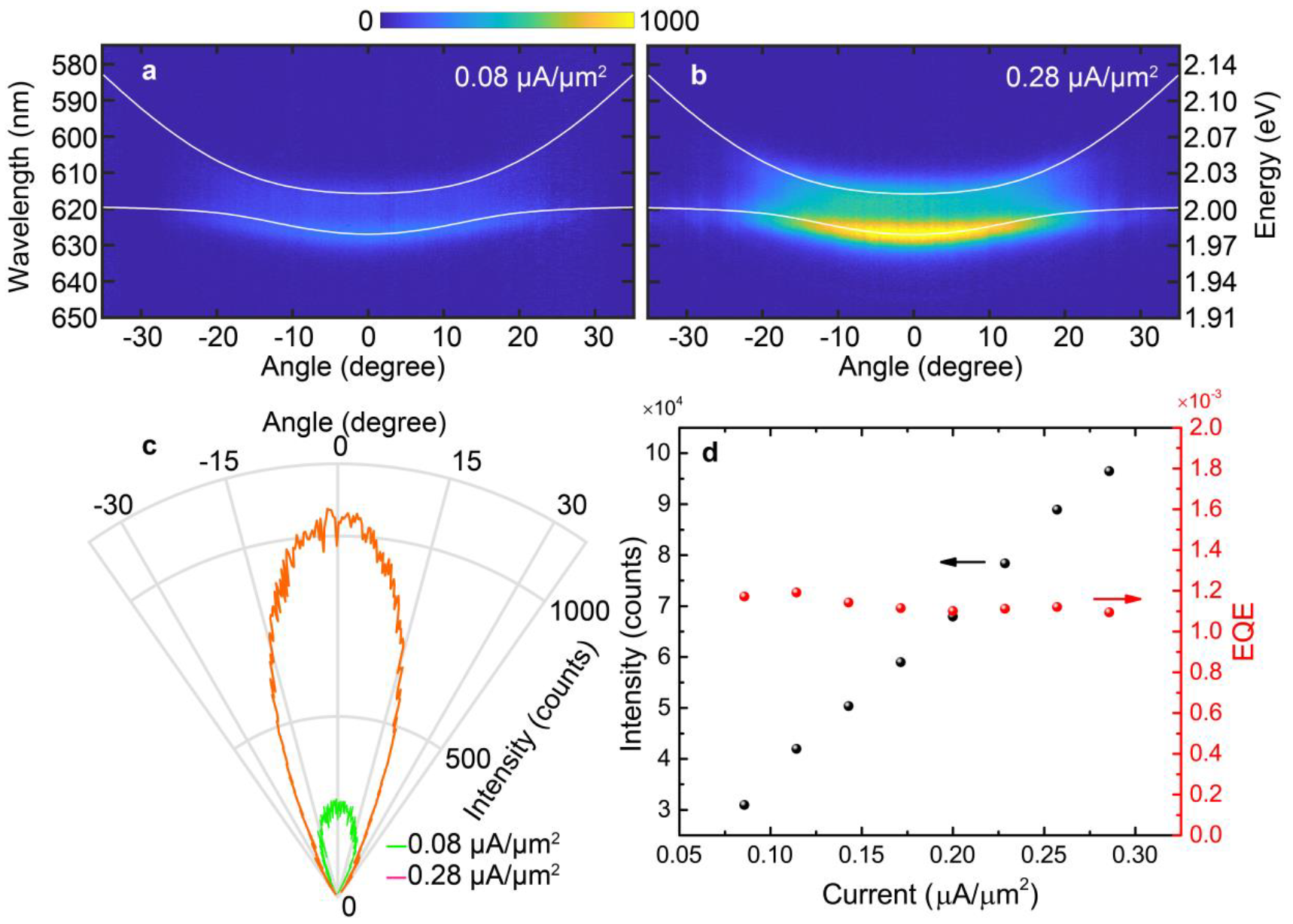
Image No. 3
As the tunneling current increases, the total EL intensity increases. A weak EL from polaritons is observed near the threshold bias ( 3a ), while at a sufficiently large bias above the threshold, polariton emission becomes distinct ( 3b ).
Figure 3c shows a polar graph of the EL intensity as a function of angle, depicting a narrow emission cone of ± 15 °. The radiation pattern remains almost unchanged for both the minimum (green curve) and maximum (orange curve) excitation current. 3d shows the integrated intensity at various moving tunnel currents, which, as can be seen from the graph, is quite linear. Consequently, increasing the current to high values can lead to successful scattering of polaritons along the lower branch and create an extremely narrow radiation pattern due to the generation of polaritons. However, it was not possible to achieve this in this experiment due to the limitation associated with dielectric breakdown of the hBN tunnel barrier.
The red dots in 3d show the measurements of another indicator - external quantum efficiency * .
Quantum efficiency * is the ratio of the number of photons, the absorption of which caused the formation of quasiparticles, to the total number of absorbed photons.The observed quantum efficiency is comparable to that in other polariton LEDs (based on organic materials, carbon tubes, etc.). It should be noted that in the studied device the thickness of the light-emitting layer is only 0.7 nm, while for other devices this value is much higher. Scientists do not hide the fact that the quantum efficiency of their device is not the highest, but it can be increased by placing a larger number of monolayers inside the tunnel zone, separated by thin layers of hBN.
The researchers also tested the effect of cavity mismatch on the EL of a polariton by fabricating another device, but with a stronger mismatch (-43 meV).

Image No. 4
Image 4a shows EL spectra with an angular resolution of such a device at a current density of 0.2 μA / μm 2 . Due to severe detuning, the device shows a pronounced effect of a bottleneck in EL with a maximum emission occurring at a large angle. This is further confirmed in image 4b , where the polar graphs of this device are compared with the first ( 2c ).
For a more detailed acquaintance with the nuances of the study, I recommend that you look into the report of scientists .
Epilogue
Thus, all the above observations and measurements confirm the presence of polariton electroluminescence in the vdW heterostructure embedded in the optical microresonator. The tunnel architecture of the device under study provides the introduction of electrons / holes and recombination into the WS 2 monolayer, which serves as a light emitter. It is important that the tunnel mechanism of the device does not require alloying components, which minimizes losses and various changes associated with temperature.
It was found that EL has a high directivity due to the dispersion of the resonator. Consequently, an improvement in the quality factor of the resonator and a higher current supply will increase the efficiency of microresonator LEDs, as well as electrically controlled microresonator polaritons and photon lasers.
This work once again confirmed that transition metal dichalcogenides possess truly unique properties and a very wide range of applications.
Such research and innovative inventions can greatly affect the development and dissemination of data transmission technologies through LEDs and light as such. These futuristic technologies include Li-Fi, which can provide significantly higher speed than existing Wi-Fi.
Thank you for your attention, remain curious and have a good working week, guys! :)
Thank you for staying with us. Do you like our articles? Want to see more interesting materials? Support us by placing an order or recommending it to your friends, a 30% discount for Habr users on a unique analogue of entry-level servers that was invented by us for you: The whole truth about VPS (KVM) E5-2650 v4 (6 Cores) 10GB DDR4 240GB SSD 1Gbps from $ 20 or how to divide the server? (options are available with RAID1 and RAID10, up to 24 cores and up to 40GB DDR4).
Dell R730xd 2 times cheaper? Only we have 2 x Intel TetraDeca-Core Xeon 2x E5-2697v3 2.6GHz 14C 64GB DDR4 4x960GB SSD 1Gbps 100 TV from $ 199 in the Netherlands! Dell R420 - 2x E5-2430 2.2Ghz 6C 128GB DDR3 2x960GB SSD 1Gbps 100TB - from $ 99! Read about How to Build Infrastructure Bldg. class c using Dell R730xd E5-2650 v4 servers costing 9,000 euros for a penny?
All Articles