With a good microcontroller and time flies fast or a weekend oscilloscope
Some time ago, the author of these lines undertook to develop a compact recorder of a single-polar analog signal within 3 volts with the highest possible reading speed and the lowest possible costs and sizes. In the list of the lowest possible costs, I also entered my headache and chose the well-known to me STM32F303. This, I recall, Cortex-M4 72 megahertz from a well-known company, with built-in 12 bit, quite nimble, analog-to-digital converters (ADC or ADC, as you like) and with a CAN interface on board.
Such small registrars required several dozen. And the microcontroller’s case with 48 legs inspired hope that this reader could be called compact. The CAN interface, with which I already had a good relationship, gave me the opportunity to combine all this jazz in a fairly convenient manner.
The speed with which, in the end, it all worked, turned out to be quite suitable to declare the operability of the chosen approach. It was possible to achieve a half microsecond sampling step. Headache and assembler could not be avoided, but who now recalls this?
However, some sediment remained. The thought remained that, in terms of speed, not everything was squeezed out.
And now, the STM32G4 series has recently appeared with a clock frequency of up to 170 megahertz with an option in a small case, and with almost the same fast ADCs on board in the amount of five pieces. It was necessary to do something.
Nobody was standing over the soul now and there was no need to worry about deadlines and plans.
Indeed, if you do not think about it, then you can enjoy even the work. But, frankly, I had to think about time. To think for a long time about small time (and what, poetically).
The thought suggested itself that we should start a little from the other end. That is, we must proceed from the shortest possible ADC sampling time, which, based on the description, takes 2.5 clock cycles and amounts to 62.5 nanoseconds at 40 MHz (160 MHz / 4). Then the sampling step of 100 nanoseconds suggests itself. The number is round and, most importantly, quite small and beautiful, why not try it?
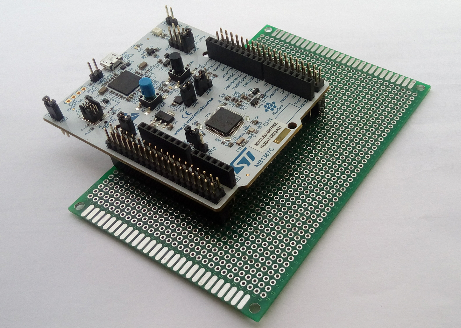
In addition, the NUCLEO-G474RE board suitable for experiments appeared on sale and was bought, to which it was reasonable to add an additional breadboard with two double-row connectors to solder all sorts of wires and parts to the breadboard and not spoil the main one. Here's how it looks ready-made.
There, below, there are several wires and a resistor with a capacitor, take my word for it.
Now you need to apply a suitable electrical signal immediately to all four ADCs, then run them one after another with a constant step (at first, when debugging, not very short). Why four? According to the description, each ADC spends 15 clock cycles or 0.025 * 15 = 375 nanoseconds (almost 400) per conversion. Therefore, at step 100, a conveyor of four ADCs is required.
An RC circuit was used as an input signal, to which voltage was simply supplied from the controller foot. I assigned this leg to control the TIM5 timer in single pulse mode.
The minimum wiring diagram looked like the image below.

ADC1-ADC4 were involved. The bit depth could be reduced for some increase in speed, but 12 bits outweighed, because I did not want to lose the accuracy of the measurements. To start each ADC in the required order and with the required step, three timers are used (TIM2, TIM3, TIM4) and another timer (TIM1) is used to synchronize the above three. Figure 2 below shows the signals around which everything is built.
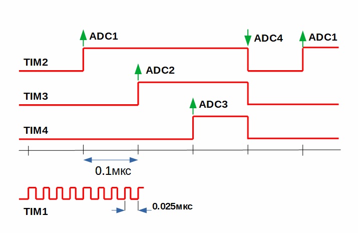
The green arrows indicate the edge of the pulses along which the respective ADC1-ADC4 converters are triggered.
To get the planned 100 nanoseconds, we had to lower the clock frequency to 160 megahertz, so that everything would be divided completely as it should. At first, the step was set much slower, 4 microseconds, to calmly check the operation of timers using interrupts, output ports and an oscilloscope. Then, by interrupt, it was debugged and earned direct access to memory. Ultimately, only one interrupt is processed - this is the interruption of the end of work from the fourth (last) channel of direct access to memory. The figure below shows the connections of the hardware units involved in the process, as well as four output memory buffers.

Of the four memory buffers (shown on the right), the samples are collected programmatically in one result buffer.
In this controller, unlike the STM32F303, there is a request switching unit (DMAMUX), which allows you to redirect a huge number of requests from peripheral devices to only 16 DMA1 channels and 16 DMA2 channels. In the Reference manual, the DMAMUX output requests are counted from 0, and the inputs of the DMA channel channels are counted from 1. I did not change it, I left it as in the original source.
A TIM5 timer is used as a single pulse generator. It provides a convenient single pulse mode. Convenience lies in the possibility of setting the time before the start of the pulse and setting the duration of the pulse itself. This impulse came out as shown below in the picture, kindly provided by a rented oscilloscope.
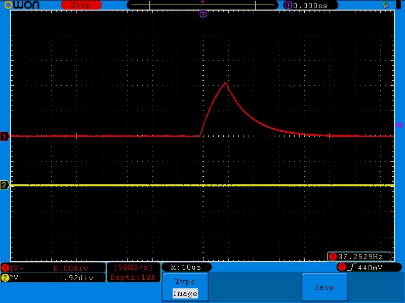
The oscillogram shows that the rise of the pulse lasts 10 microseconds, which means it should accommodate about 100 samples.
The project was done in IAR 8.4 manually (that is, without Cuba and the Ball), but, I hope, it will be understood by a variety of faiths. You can see it here .
Here is a picture of the contents of a separate ADC1 buffer and the result collected from four sources of the buffer in the region of the beginning of the input pulse.
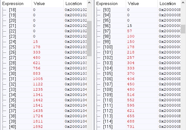
But the contents of these buffers are in the region of the peak of the pulse (where the value reaches 2508).
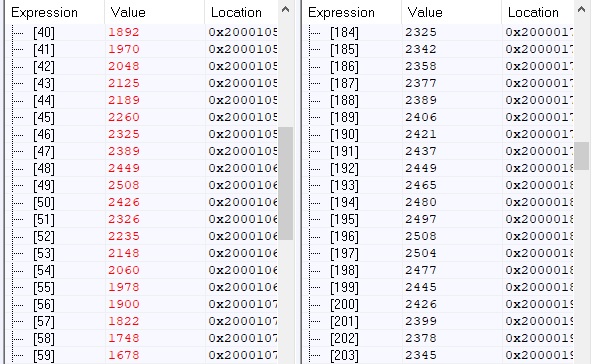
As you can see, 196-95 = 101 counts were spent on the section from the beginning of the pulse to its peak.
So the sampling rate is 10 megahertz. It didn’t work at that speed right away.
In order to achieve this, I had to stop the processor before starting direct memory access (DMA1). It's good that the Cortex-M4 has a special assembler instruction WFI (Wait for interruptions). If this is not done, then the processor will get in the way under the DMA's feet and occupy the bus with memory accesses that may well wait.
If you increase the counting step to 200 nanoseconds, then they will stop pushing and heal peacefully and happily.
If we involve the COMP4 comparator in its work and connect its positive input (port PB0) with the input signal, then use the DAC (DAC1) and connect its output (CH1) with the negative input of the comparator (inside the controller), we get a threshold device with an adjustable threshold. Interruptions from the operation of the comparator will allow you to start the general clock timer TIM1 and get a standby mode, as in an oscilloscope.
All Articles