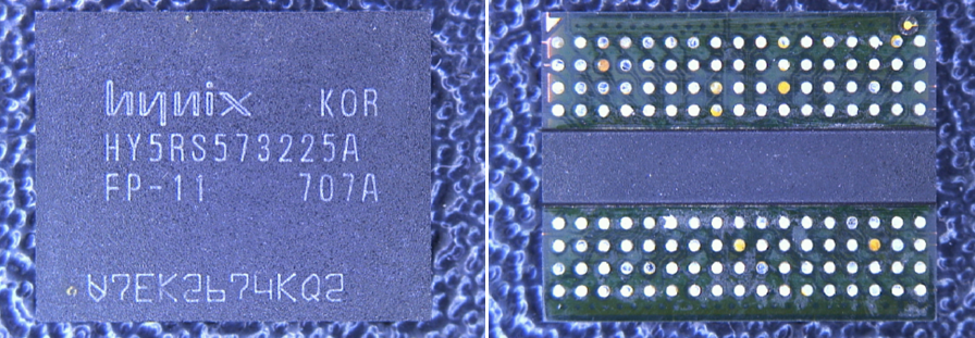
The experimental memory was removed from the GT8800 video card in the amount of 10 pieces of memory chips of 32 MB each. Appearance of the sample for study. On the one hand, the IC is covered with plastic, on the other hand, textolite with a plastic groove.
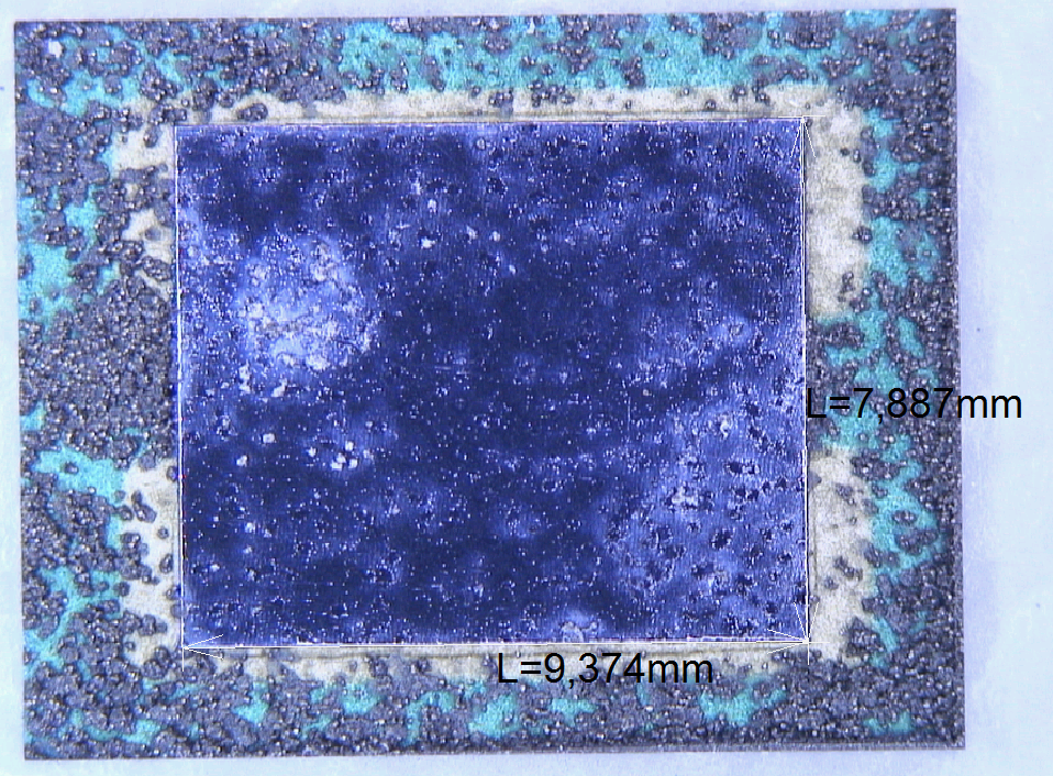
Remove the top layer of plastic. Under it, a crystal of ~ 9.4 x 8 mm in size is detected. The plastic filler is made of glass balls of approximately the same diameter.
The crystal is upside down and the topology is on the back of the crystal. The crystal itself is planted on a light brown compound. It is very similar to silicone sealant, only more elastic. We remove the plastic groove from the back of the crystal.
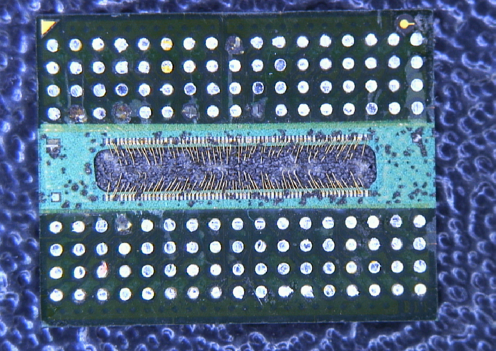
A groove is hidden in the groove, which is honestly made with gold wire. An interesting solution is the location of the pads in the middle of the crystal. This is most likely due to the fact that the crystal is turned upside down, and therefore it would be more difficult to weld it onto a textolite with pads around the perimeter - more cuts would be required on the textolite. There is a memory in which the crystal is soldered to microspheres, and such a memory operates at higher frequencies. Such a memory does not have a plastic groove at the bottom, the presence of which indicates a wire unwrap hidden there.
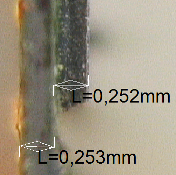
The sizes of the thickness of the crystal and textolite are about 250 μm, respectively. It is very easy to break such a crystal, so the removal of the crystal took a long time, it was difficult, nervous and it turned out far from the first time. It is good that the memory was not in a single copy.
We remove the removed crystal from the compound (sealant).
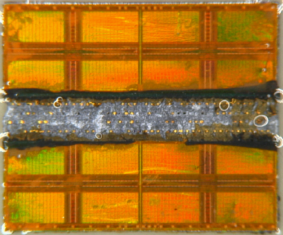
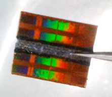
This is the top 32 MB crystal topology. The topology of memory is repetitive. In it you can see many identical repeating rectangular areas of different sizes. The topology seems to be mirrored horizontally and vertically.
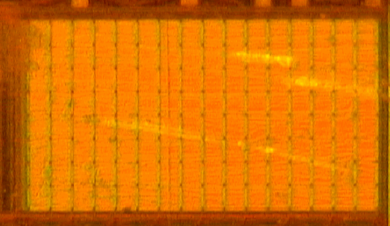
If you approach one of these rectangular areas, then you can still see the same square blocks in it. Approximation 40X.
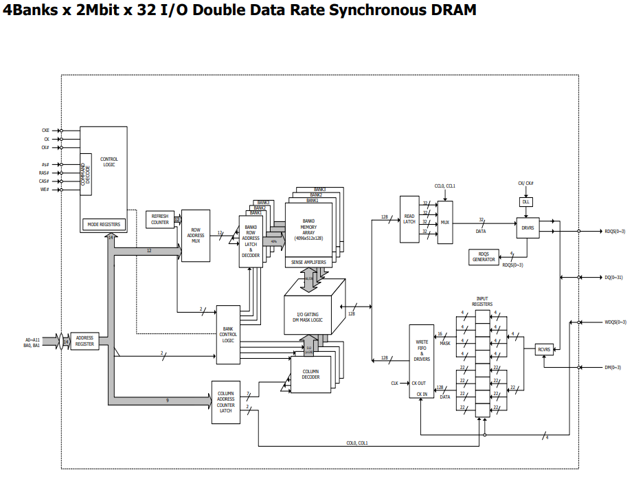
Organization of memory from a data shield. Memory is an array of arrays. In it, rows and columns are combined into memory banks, and they, in turn, form arrays of cans. These are all repeating structures.
Arrays are combined by buses, through which the supply voltage and data are delivered. Approximation 400X. Clickable.
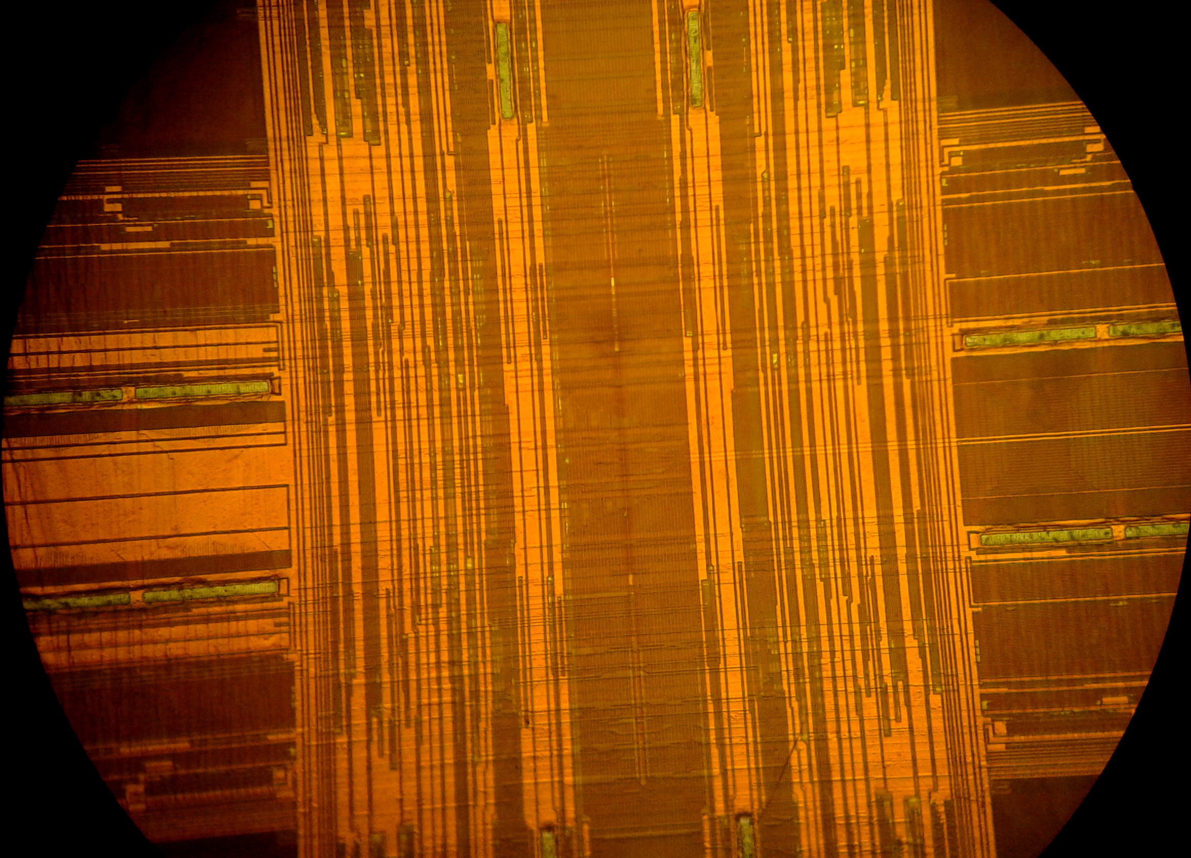
I am not allowed to conduct further analysis of the topology with equipment and knowledge. But somewhere there, in the depths of the layers are millions of microscopic capacitors and transistors. Approximation 400X. Clickable.

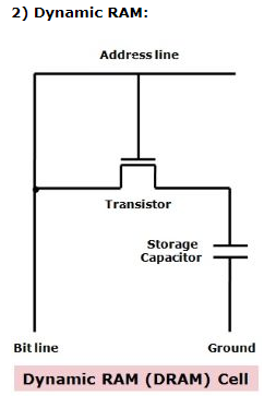
RAM cell DRAM. It consists of a transistor and a capacitor.
Conclusion: The crystals of RAM are quite large in area, and this applies to the entire SDRAM of the memory, from DDR1 to DDR6, and this eats up the silicon budget of the wafer and plays an important role in shaping its value. Thanks to the engineers for the maximum reduction in cost of the assembly - the use of PCB, plastic, etc. The memory capacities are also impressive. Now you can’t surprise anyone with gigabytes of memory - we are used to it.