Placing bare chipsets on a silicon network will allow you to make smaller computers and more processing power

The need to make certain devices less and less, while others more and more, has long been the main motivator for innovation in electronics. The first option manifests itself in progress from laptops to smartphones, then to smart watches, smart headphones and other “invisible” electronics. The second option determines the configuration of modern data centers - megawatt monsters that fill storage facilities specially built for them around the world. Interestingly, in both cases, progress is limited by the same technology - only for various reasons.
We claim that the PCB is the culprit. Our solution is to completely get rid of it.
Our study shows that printed circuit boards can be replaced with the same material that the chips soldered to it consist of - that is, silicon. Such an approach would make it possible to create both systems of smaller size and weight, suitable for wearable electronics and other devices of limited size, and incredibly powerful high-speed computers, capable of shoving the computing power of a dozen servers into a silicon substrate the size of a dinner plate.
This fully silicon technology, which we call the silicon interconnect network, allows you to connect bare chips directly to individual silicon fragments. Unlike tracks on printed circuit boards, the contact between the chips on our substrate is the same size as the tracks inside the chips. In this regard, much more connections can be laid in the substrate, and all of them are capable of transmitting data faster with less power consumption.
The silicon-interconnect fabric (Si-IF) offers another added benefit. This is a great way to break up the relatively large, complex and uncomfortable single-chip systems [system-on-a-Chip, SoC], on which everything today rests, from smartphones to supercomputers. Instead of SoC, system developers could use conglomerates of smaller, easier to design and manufacture chipsets that are closely interconnected on Si-IF. Such a revolution of chipsets is already underway - AMD, Intel, Nvidia and other companies are offering chipset sets assembled inside advanced cases. An interconnect silicon network extends this idea by breaking the system case and allowing you to include the entire computer in it.
To understand the full benefit of eliminating a circuit board, consider what happens with a typical SoC. Due to the development of electronics according to Moore's law, on a square centimeter of silicon, you can pack almost everything you need for a smartphone to work. Unfortunately, for many reasons related to the features of the printed circuit board, this piece of silicon is placed inside a plastic case, sometimes 20 times the size of the chip itself.
The difference in size between the chip and the case creates at least two problems. Firstly, the weight and volume of a packed chip is greater than that of a piece of silicon itself. Obviously, this is a problem for all devices that need to be small, thin and light. Secondly, if a finished product requires several chips that exchange data with each other (and most systems have one), then the distance that the signal needs to cover increases by more than 10 times. This is a bottleneck for speed and power consumption, especially when exchanging large amounts of data. This is probably the biggest challenge for implementing data-dependent applications — graphics, machine learning, and search. Even worse, chips in such cases are harder to cool. For several decades, heat dissipation has been a limiting factor for electronics.
But if these cases are so problematic, why not get rid of them? Because of the circuit board.
The task of the printed circuit board is to combine chips, passive components and other devices into a working system. But this technology is not perfect. Printed circuit boards are hard to make perfectly even - they often bend. Chip bodies are usually connected to the board using droplets of solder, which melt and re-solder during production. Limitations of soldering technology together with surface curvature cause droplets to not be closer than 0.5 mm to each other. In other words, it will be possible to place no more than 400 contacts per square centimeter. For many applications, this is too little for power and signal transmission to and from the chip. For example, on a small surface occupied by the crystal of the Intel Atom processor there is enough space for hundreds of contacts with a size of 0.5 mm, and it needs 300. Developers use cases for crystals so that the mathematics converge with the number of contacts per unit area. The case takes tiny contacts of a silicon chip - from 1 to 50 microns wide - and extends them to the board scale, 500 microns.
Recently, the semiconductor industry has tried to limit the problems associated with printed circuit boards by developing advanced enclosures with silicon interposer technology. Interposer is a thin layer of silicon on which a small number of bare silicon chips are attached, connected to each other through a large number of contacts. But at the same time, the interposer with its chips still needs to be hidden in the case and placed on the printed circuit board, so this option adds complexity without solving the remaining problems. In addition, interposers are necessarily thin, fragile and limited in size - which means that it is difficult to create large systems on them.
We believe that the best option would be to completely get rid of cases and printed circuit boards by attaching the chips to a relatively thick (from 500 microns to 1 mm) silicon substrate. Processors, memory crystals, RF chipsets, voltage control modules, and even passive components such as inductors and capacitors can be attached directly to silicon. Compared with the usual material of printed circuit boards - fiberglass and epoxy composition FR-4 - the silicon substrate is solid and can be polished to an almost perfect plane, so curvatures are not a problem for it. Moreover, since the chips and the substrate will expand and contract when the temperature changes by the same amount, you no longer need a large and flexible connection between the chip and the substrate, such as soldering.
Solder drops can be replaced with micrometer copper pins embedded in the substrate. Using thermocompression - in fact, the precise application of heating and pressure - the copper input / output contacts of the chips can be directly connected to the pins. Thorough optimization of the thermocompression joint can give us much more reliable contacts than soldering, and at the same time using fewer different materials.
By eliminating the printed circuit boards and their weak points, it will be possible to arrange the input / output ports at a distance of only 10 microns from each other instead of 500 microns. As a result, it will be possible to place 2500 times more ports on a silicon chip without the need to use a case.
Even better, the standard semiconductor manufacturing process can be reconfigured to fabricate multi-level Si-IF wiring diagrams. Their tracks can be made much thinner than on printed circuit boards. They can be separated by only 2 microns, and not 500 microns, as on printed circuit boards. The technology even allows you to place chips at a distance of 100 microns from each other, unlike printed circuit boards, where it should be more than 1 mm. As a result, the Si-IF system saves space, energy and signal travel time.
Moreover, unlike printed circuit boards and materials for IC cases, silicon conducts heat quite well. Radiators can be mounted on both sides of the Si-IF to remove even more heat - according to our estimates, 70% more. And the more heat is removed, the faster the processors can work.
Although silicon has good tensile strength and toughness, it is slightly brittle. Fortunately, the semiconductor industry has developed methods for working with large silicon substrates to prevent cracking over several decades. And after all the necessary Si-IF production procedures, we expect them to pass most of the reliability tests, including impact testing, cyclic heating and environmental exposure.
There is no getting away from the fact that crystalline silicon is more expensive than FR-4. Although the cost depends on many factors, the price per square millimeter of an 8-layer printed circuit board can be ten times lower than that of a 4-layer Si-IF. However, our analysis shows that if you subtract the cost of placing the chips in the cases and the complex production of the boards, and take into account the space savings using Si-IF technology, the difference in cost will be insignificant, and in some cases Si-IF may even be more profitable.

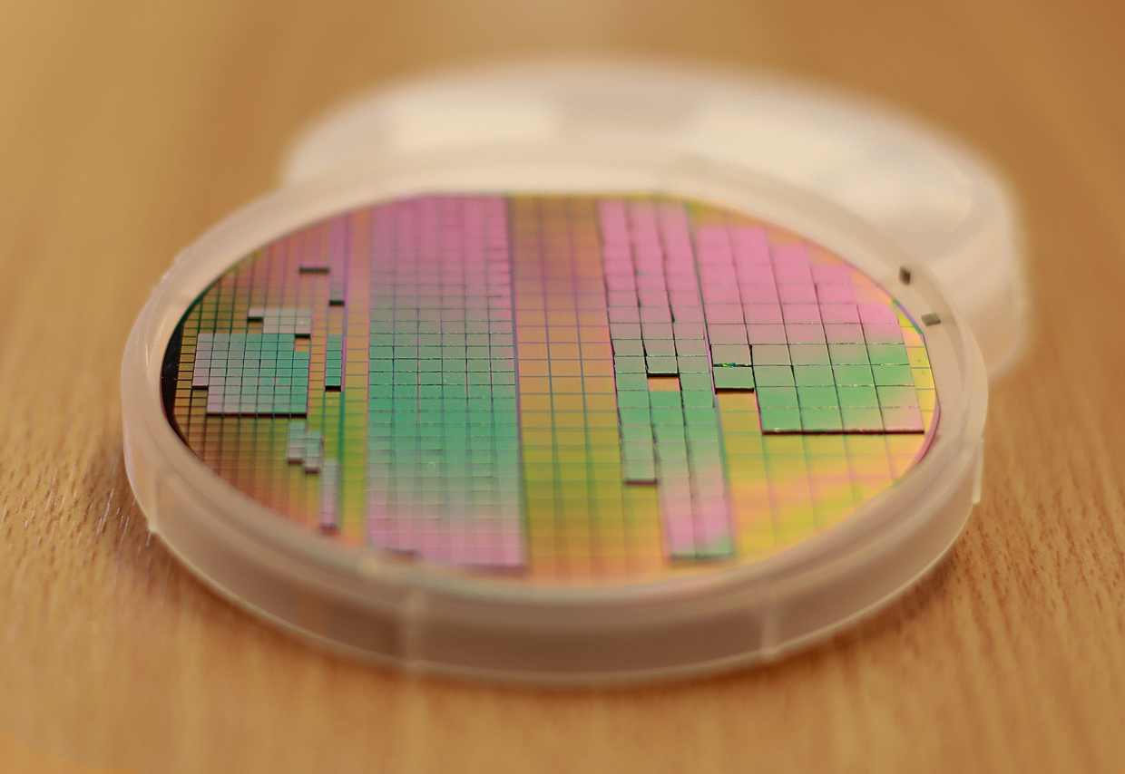
Inter-component silicon network compared to the printed circuit board and chips in the chassis. At the bottom of the diagram is an approximate scale for understanding the difference in size.
Let's look at a few examples of the benefits of using Si-IF to a computing system. In one study of server designs, we found that using chassisless processors with Si-IF can double the performance of conventional processors due to improved connectivity and increased energy dissipation. In addition, the size of the silicon “board” (in the absence of a better term) can be reduced from 1000 cm 2 to 400 cm 2 . Such a serious decrease will significantly affect the volume of data center buildings and the size of the cooling infrastructure. As for the other end of the scale, we studied a small system for the “Internet of things” based on the Arm microcontroller. In this case, the use of Si-IF reduces not only the board size by 70%, but also its weight, from 20 to 8 grams.
In addition to reducing existing systems and increasing productivity, Si-IF will allow developers to create computers that would otherwise be impossible to construct - or it would be very impractical.
In a typical powerful server, the board costs 2-4 processors. Some projects with high computational load require multiple servers. When moving data between different processors and boards, delays and bottlenecks occur. But what if all the processors were placed on a single silicon substrate? They could be integrated so tightly that the whole system would work as one large processor.
This concept was first proposed by Gene Amdahl at his Trilogy Systems company. But Trilogy did not succeed, because their production process was not able to produce sufficient quality for a working system. When manufacturing a chip, there is always the possibility of defects, and with an increase in its area, the probability of marriage increases exponentially. When the size of the chip is comparable to a dinner plate, the presence of a marriage that kills the entire system in it is almost guaranteed.
But if you have a silicon interconnect network, you can start with the chipsets that we can already produce without defects, and then combine them into a single system. Our team of researchers from the University of California at Los Angeles and the University of Illinois at Urbana-Campaign developed such a system with a substrate containing 40 GPUs. In simulations, it accelerated calculations by more than 5 times, and consumed energy by 80% less than the equivalent system of 40 GPUs created using advanced multi-chip cases and printed circuit boards.
The results were convincing, although the task was not easy. We had to take into account many restrictions, in particular: the maximum amount of heat removed from the substrate; how to make the GPU exchange data as quickly as possible; how to supply power over the entire area of the substrate.
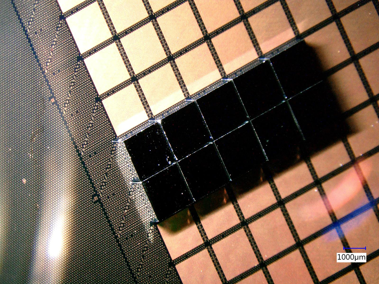
Dilets, or chipsets, integrated on an interconnected silicon network, a 100 mm substrate. Dilets, unlike chips on a printed circuit board, can be placed at a distance of 100 microns from each other
The main limitation was nutrition. With a standard chip operating voltage of 1 V, the thin tracks of the substrate would have to consume 2 kW. Instead, we raised the voltage to 12 V, reducing the current and power in this way. To do this, it was necessary to distribute the voltage regulators and capacitors across the entire substrate, and they took the place that otherwise could be given to additional GPUs. Inspired by the early results, we are now assembling a prototype computing system that we hope to complete by the end of 2020.
The silicon interconnect network can play a role in an important trend in the computer industry: the division of SoC into integrated sets of daylets [dielet - from “die”, crystal, and “–let”, reduction prefix / approx. transl.], or chiplets (we prefer to call them daylets, as this emphasizes their essence as bare silicon crystals, their small size and, possibly, incomplete functionality without other Si-IF daylets). Over the past two decades, the desire to increase performance and reduce cost has convinced developers to replace chip sets with even larger integrated SoCs. And, despite their advantages, SoC have a sufficient number of disadvantages.
Firstly, SoC is one large chip, and, as already mentioned, it is quite difficult to achieve acceptable indicators of the percentage of rejects in the production of a large chip, especially in advanced semiconductor industries (recall that the percentage of rejects exponentially increases with increasing chip area). Another drawback of SoC is the high cost of designing and starting production; for example, in the USA, a photolithographic mask can cost from $ 2 million, which makes the SoC option unavailable for most schemes. Moreover, any, even a small change in the scheme or updating the production process will require significant processing of the entire SoC. Finally, the SoC approach tries to fit all the subsystems into one production process, even when some of these subsystems could be done better in another process. As a result, nothing in SoC reaches the highest possible efficiency or speed.
Integration on Si-IF without the participation of enclosures avoids all these problems, while maintaining the small size and speed of SoC, while giving advantages in development and cost. It breaks down SoC into its constituent components and recreates a system on a substrate, system – on – Si-IF (SoIF).
Such a system consists of independently produced daylets, connected via Si-IF. The minimum distance separating dilets (tens of micrometers) is comparable to the distance between two SoC function blocks. The wiring on Si-IF is the same as that used at the upper level of SoC, so the density of the compounds is comparable.
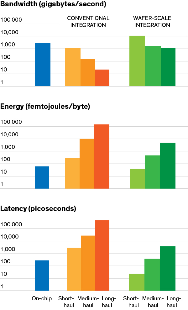
From top to bottom: bandwidth (GB / s), power consumption (fJ / B), delay (ps).
Blue - system on a chip, shades of red - normal integration, shades of green - system-on-substrate
The advantages of SoIF over SoC are due to the size of the delay. Small deletes are cheaper to produce than large SoCs because they have a lower reject rate due to their small size. In SoIF, only the substrate itself has a large size. But she is unlikely to have a problem with the marriage, since it is made of several layers that are easy to manufacture. Most of the loss due to defects is due to defects in the transistor layers or in the superdense lower metal layers, which is the case with an interconnected silicon network.
In addition, SoIF will have all the advantages in the pursuit of which the industry is switching to chipsets. For example, the transition of SoIF to the next manufacturing process should be easier and cheaper. Each dylet can have its own production technology, and only those dylets that really require it can be updated. And the delay factors, which are not particularly beneficial from the reduction of transistors, will not need to be changed. Such heterogeneous integration allows you to create a completely new class of systems that mix the shutters of different generations and technologies that are usually not compatible with CMOS. For example, our group recently demonstrated the combination of an indium phosphide crystal with SoIF as an example of potential use in high frequency circuits.
Since the dilettes will be produced and verified before connecting to SoIF, they can be used in different systems, which will significantly save on them. As a result, the total cost of developing and manufacturing SoIF may be 70% lower than that of SoC. This will be especially true for large systems produced in small batches - as is the case with the aerospace and defense industries, where there is demand only for batches of the order of several hundred or thousand units. Custom-made systems will also be easier to do at SoIF, as this reduces both cost and development time.
We believe that such cost and diversity benefits can lead to the start of a new era of innovation in which new hardware will be available to a much larger number of designers, startups and universities.
In the past few years, we have made significant progress in Si-IF integration technology, but much remains to be done. First of all, it is necessary to show a commercially viable low-defective Si-IF production process.Creating Si-IF-scale substrates may require innovation in maskless lithography. Most lithographic systems that exist today can make substrates measuring 33x24 mm. As a result, we need a system capable of delivering a substrate with a diameter of 300 mm.
We also need mechanisms for checking naked daylets and Si-IF. The industry is already moving towards testing bare crystals as chip makers switch to cheatlets in advanced packages and three-dimensional integration.
Then we need new radiators or other heat dissipation strategies that take advantage of the good thermal conductivity of silicon. My colleagues at the University of California and I are developing an integrated substrate cooling and nutrition solution called PowerTherm.
In addition, for the assembly of complete systems, you will need frames, fasteners, connectors and cables.
We will also need to make a few changes to the development methodology so that one of SoIF promises becomes a reality. Si-IF is a passive substrate in which there are only one conductors. Therefore, inter-flight connections should be short. For longer tracks connecting far located dilets, we will need intermediate dilets that transfer data further down the chain. It will be necessary to review the design algorithms responsible for the arrangement of elements and the purpose of contacts so that they take full advantage of this type of integration. And we will also need to develop new ways to explore various system architectures that take advantage of the heterogeneity and updatability of SoIF.
We will also need to consider the reliability of the systems. If a dylet is found to be defective after attaching it or fails during operation, it will be very difficult to replace it. Therefore, in SoIF, especially in large ones, it will be necessary to build fault tolerance. It can be implemented at the network level or at the dayleet level. At the network level, it will be necessary to ensure the passage of the signal bypassing the failed daylets. At the daylet level, it will be possible to consider various tricks with physical redundancy, for example, the use of several copper pins for each of the input / output ports.
Of course, the advantages of a daylet assembly depend on the availability of useful daylets that can be integrated into the system. So far, the industry is dealing with what kind of dilets to produce. You can’t just do a daylet for each subsystem in SoC, as some of the daylets will be too tiny. One promising approach is the use of statistical processing of existing SoC circuits and printed circuit boards in order to find functions that "tend" to be physically closer to each other. If these functions have the same production technologies and update cycles, then they need to be integrated into a single daylet.
This list of problems may seem very long, but researchers are already working on some of them as part of the Defense Advanced Research Projects Agency's Common Heterogeneous Integration and IP Reuse Strategies (CHIPS) program, as well as with industry consortia. And if we can solve these problems, it will seriously help us maintain the legacy of Moore’s law in a smaller, faster, and cheaper way.