“Mutation is the key to unraveling the mysteries of evolution. The development path from the simplest organism to the dominant biological species has been going on for millennia. But every hundred thousand years in evolution, there is a sharp leap forward ”(Charles Xavier, X-Men, 2000). If we discard all the sci-fi elements that are present in comics and films, then the words of Professor X are quite true. The development of something proceeds uniformly most of the time, but sometimes jumps occur that have a huge impact on the whole process. This applies not only to the evolution of species, but also to the evolution of technology, the main engine of which is people, their research and inventions. Today we will meet with you a study that, according to its authors, is a real evolutionary leap in nanotechnology. How did scientists from Northwestern University (USA) manage to create a new two-dimensional heterostructure, why were graphene and borofen chosen as the basis, and what properties can such a system have? The report of the research group will tell us about this. Go.
Study basis
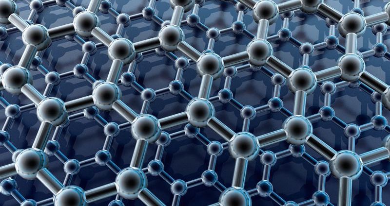
The term "graphene" we have heard many times - this is a two-dimensional modification of carbon, consisting of a layer of carbon atoms with a thickness of 1 atom. But Borofen is extremely rare. This term refers to a two-dimensional crystal consisting solely of boron atoms (B). For the first time, the possibility of the existence of borofen was predicted back in the mid-90s, but in practice, this structure was obtained only by 2015.
The atomic structure of borofen consists of triangular and hexagonal elements and is a consequence of the interaction between two-center and multicenter intra-plane bonds, which is very characteristic of elements with an electron deficiency, which includes boron.
* By two-center and multicenter bonds we mean chemical bonds - interactions of atoms characterizing the stability of a molecule or crystal as a single structure. For example, a two-center two-electron bond occurs when 2 atoms divide 2 electrons among themselves, and a two-center three-electron bond - 2 atoms and 3 electrons, etc.From a physical point of view, borofen can be more durable and flexible than graphene. It is also believed that borofen structures can be an effective addition to batteries, since borofen has a high specific capacity and unique properties of electronic conductivity and ion transfer. However, at the moment this is only a theory.
Being a trivalent element * , boron has at least 10 allotropes * . In two-dimensional form, a similar polymorphism * is also observed.
The trivalent element * is capable of forming three covalent bonds, the valency of which is three.
Allotropy * - when one chemical element can be represented as two or more simple substances. As an example, carbon is diamond, graphene, graphite, carbon nanotubes, etc.
Polymorphism * - the ability of a substance to exist in different crystalline structures (polymorphic modifications). In the case of simple substances, this term is synonymous with allotropy.Given such a wide polymorphism, the assumption arises that borofen may be an excellent candidate for creating new two-dimensional heterostructures, since various configurations of boron bonds should weaken the requirements for matching the crystal lattice. Unfortunately, earlier this question was studied exclusively at the theoretical level due to difficulties in the synthesis.
For conventional 2D materials obtained from bulk layered crystals, vertical heterostructures can be realized using mechanical styling. On the other hand, two-dimensional lateral heterostructures are based on upward synthesis. Atomically accurate lateral heterostructures have great potential in solving problems with controlling the functionality of a heterojunction, however, due to covalent bonding, imperfect lattice matching usually leads to wide and disordered interfaces. Therefore, there is potential, but there are also problems in its implementation.
In this work, researchers were able to integrate borofen and graphene into one two-dimensional heterostructure. Despite the mismatch between the crystallographic lattices and the symmetry between borofen and graphene, the sequential deposition of carbon and boron on an Ag (111) substrate in ultrahigh vacuum (UHV) leads to almost atomically accurate lateral heterointerfaces with predicted lattice alignments, as well as vertical heterointerfaces.
Study preparation
Before studying the heterostructure, it was necessary to fabricate it. The growth of graphene and borofen was carried out in an ultrahigh vacuum chamber with a pressure of 1x10 -10 mbar.
The single-crystal Ag (111) substrate was purified by repeated sputtering cycles of Ar + (1 x 10 -5 mbar, energy 800 eV, 30 minutes) and thermal annealing (550 ° , 45 minutes) to obtain an atomically clean and flat surface of Ag (111 )
Graphene was grown by electron beam evaporation of a pure (99.997%) graphite rod 2.0 mm in diameter onto an Ag (111) substrate heated to 750 ° C at a filament current of ~ 1.6 A and an accelerating voltage of ~ 2 kV, which gives an emission current of ~ 70 mA and a carbon flux of ~ 40 nA. The pressure in the chamber was 1 x 10 -9 mbar.
Borofen was grown by electron beam evaporation of a pure (99.9999%) boron rod onto a submonolayer graphene heated to 400-500 ° on Ag (111). The glow current was ~ 1.5 A, and the accelerating voltage was 1.75 kV, which gives an emission current of ~ 34 mA and a boron flux of ~ 10 nA. The pressure in the chamber during borofen cultivation was approximately 2 x 10 -10 mbar.
Research results
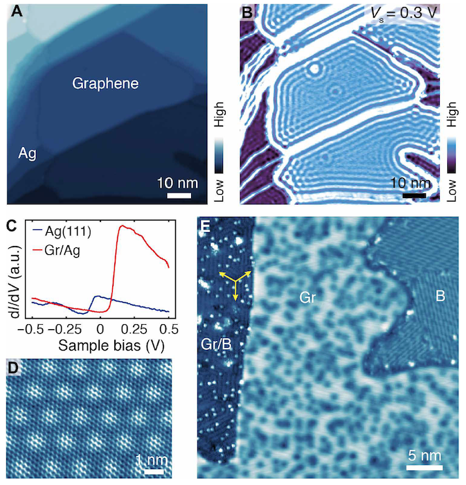
Image No. 1
Image 1A shows a STM * image of grown graphene, where graphene domains are best visualized using a dI / dV map ( 1B ), where I and V are the tunneling current and sample displacement, and d is the density.
STM * - scanning tunneling microscope.The dI / dV maps of the sample allowed us to see a higher local density of states of graphene in comparison with the Ag (111) substrate. In accordance with previous studies, the surface state of Ag (111) has a stepwise characteristic shifted toward positive energies in the dI / dV spectrum of graphene ( 1C ), which explains the higher local density of states of graphene by 1 V at 0.3 eV.
In the 1D image, we can see the structure of single-layer graphene, where the honeycomb lattice and the moire superstructure * are clearly visible * .
Superstructure * is a feature of the structure of a crystalline compound that repeats at a certain interval and thus creates a new structure with a different alternation period.At lower temperatures, growth leads to the formation of dendritic and defective graphene domains. Due to weak interactions between graphene and the underlying substrate, the rotational alignment of graphene with respect to underlying Ag (111) is not unique.
Moire * - overlay of two periodic mesh patterns on each other.
After boron deposition, scanning tunneling microscopy ( 1E ) showed the presence of a compound of borofen and graphene domains. Also visible in the image are the areas inside graphene, which were later identified as graphene intercalated with borofen (indicated in the image Gr / B ). In this area, linear elements are also clearly visible, oriented in three directions and separated by an angle of 120 ° (yellow arrows).
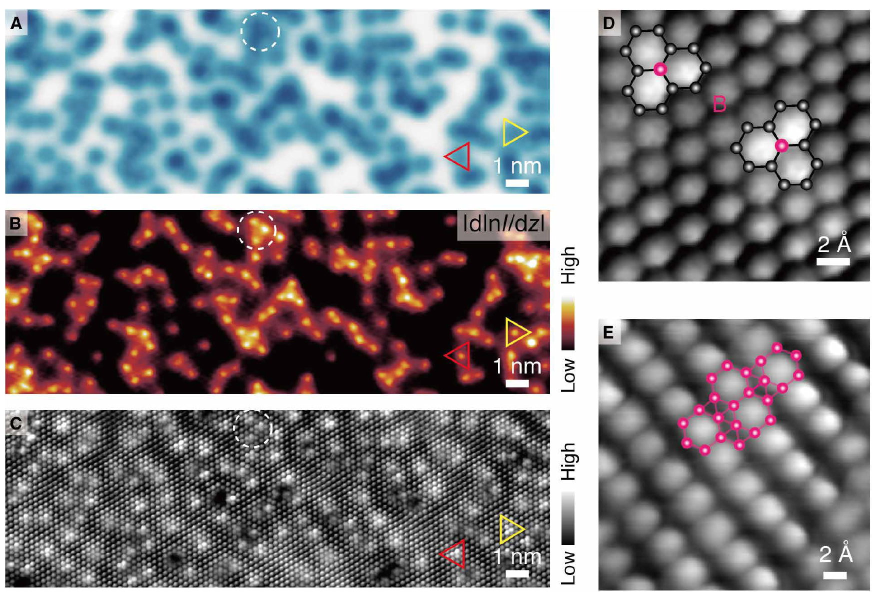
Image No. 2
The image on 2A , like 1E , confirms the appearance of localized dark depressions (depressions) in graphene after boron deposition.
In order to better examine these formations and find out their origin, another picture was taken of the same area, but with the use of maps | dln I / dz | (2B), where I is the tunneling current, d is the density, and z is the separation of the probe-sample (the gap between the microscope needle and the sample). Application of this technique allows obtaining images with high spatial resolution. You can also use CO or H 2 on a microscope needle.
Image 2C is a CTM image whose needle was coated with CO. Comparison of images A , B and C shows that all atomic elements are defined as three adjacent bright hexagons directed in two nonequivalent directions (red and yellow triangles in the images).
Enlarged images of this region ( 2D ) confirm that these elements are in agreement with the dopants of boron, which occupy two graphene sublattices, as indicated by superimposed structures.
The CO coating of the microscope needle made it possible to reveal the geometric structure of the borofen sheet ( 2E ), which would not have been possible if the needle was standard (metal) without CO coating.
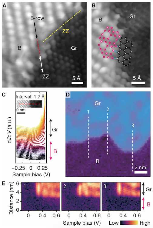
Image No. 3
The formation of lateral heterointerfaces between borofen and graphene ( 3A ) should occur when borofen grows near graphene domains in which boron is already present.
Scientists recall that lateral heterointerfaces based on graphene-hBN (graphene + boron nitride) have lattice matching, and heterojunctions based on transition metal dichalcogenides have symmetry matching. In the case of graphene / borophene, the situation is slightly different - they have minimal structural similarity in terms of lattice constants or crystal symmetry. However, despite this, the graphene / borofen lateral heterointerface shows almost perfect atomic consistency, with the directions of the boron row (B-row) aligned with the zigzag (ZZ) directions of graphene ( 3A ). Figure 3B shows an enlarged image of the ZZ region of the heterointerface (blue lines indicate interfacial elements corresponding to boron-carbon covalent bonds).
Since borofen growth occurs at a lower temperature compared to graphene, the edges of the graphene domain are unlikely to have high mobility during the formation of a hetero interface with borofen. Therefore, an almost atomically precise heterointerface is probably the result of various configurations and characteristics of multicenter boron bonds. The spectra of scanning tunneling spectroscopy ( 3C ) and differential tunneling conductivity ( 3D ) show that the electronic transition from graphene to borophene occurs at a distance of ~ 5 Å without visible interface states.
Image 3E shows three spectra of scanning tunneling spectroscopy taken along three dashed lines in 3D, which confirm that this short electronic transition is insensitive to local interfacial structures and is comparable to that at borofen-silver interfaces.
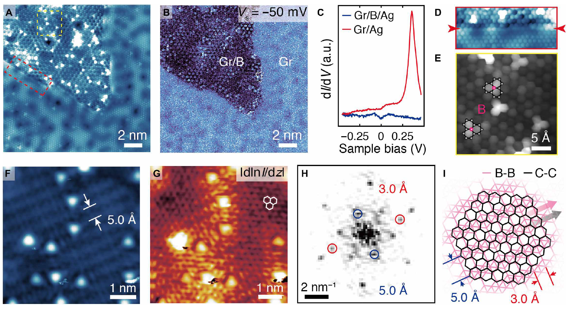
Image No. 4
Graphene intercalation * has also been extensively studied before, however, the conversion of intercalants into true 2D sheets is relatively rare.
Intercalation * - the reversible inclusion of a molecule or group of molecules between other molecules or groups of molecules.The small atomic radius of boron and the weak interaction between graphene and Ag (111) suggest a possible intercalation of graphene with boron. Figure 4A provides evidence of not only boron intercalation, but also the formation of vertical borophene-graphene heterostructures, especially triangular domains surrounded by graphene. The honeycomb lattice observed on this triangular domain confirms the presence of graphene. However, this graphene exhibits a lower local density of states at -50 meV compared to surrounding graphene ( 4V ). Compared to graphene directly on Ag (111), the absence of signs of a high local density of states in the dI / dV spectrum ( 4C , blue curve) corresponding to the surface state of Ag (111) is the first evidence of boron intercalation.
Also, as expected for partial intercalation, the graphene lattice remains continuous along the entire lateral interface between graphene and the triangular region ( 4D - corresponds to the rectangular region at 4A , circled in red dotted line). A picture using CO on a microscope needle also confirmed the presence of boron substitutional impurities ( 4E - corresponds to a rectangular region of 4A surrounded by a yellow dotted line).
Microscope needles without any coating were also used during the analysis. In this case, signs of one-dimensional linear elements with a frequency of 5 Å ( 4F and 4G ) were revealed in intercalated graphene domains. These one-dimensional structures resemble boron rows in the borofen model. In addition to the set of points corresponding to graphene, the Fourier transform of the image on 4G displays a pair of orthogonal points corresponding to a rectangular lattice of 3 Å x 5 Å ( 4H ), which is in excellent agreement with the borofen model. Moreover, the observed triple orientation of the lattice of linear elements ( 1E ) is in good agreement with the same prevailing structure observed for borofen sheets.
All these observations convincingly indicate intercalation of graphene with borofen near the edges of Ag, which, therefore, leads to the formation of vertical borofen-graphene heterostructures, which can be predominantly realized by increasing the initial graphene coating.
4I is a schematic representation of a 4H vertical heterostructure, where the direction of the boron row (pink arrow) is closely aligned with the zigzag direction of graphene (black arrow), thereby forming a rotationally proportional vertical heterostructure.
For a more detailed acquaintance with the nuances of the study, I recommend that you look into the report of scientists and additional materials to it.
Epilogue
This study showed that borofen is quite capable of forming lateral and vertical heterostructures with graphene. Such systems can be used in the development of new types of two-dimensional elements used in nanotechnology, flexible and wearable electronics, as well as in new types of semiconductors.
Researchers themselves believe that their development can be a powerful impetus for technology related to electronics. However, it is difficult to say for sure that their words will become prophetic. At the moment, much remains to be explored, understood and invented so that the science fiction ideas that fill the minds of scientists become a full-fledged reality.
Thank you for your attention, remain curious and have a good working week, guys. :)
Thank you for staying with us. Do you like our articles? Want to see more interesting materials? Support us by placing an order or recommending it to your friends, a 30% discount for Habr users on a unique analog entry-level server that we invented for you: The whole truth about VPS (KVM) E5-2650 v4 (6 Cores) 10GB DDR4 240GB SSD 1Gbps from $ 20 or how to divide the server? (options are available with RAID1 and RAID10, up to 24 cores and up to 40GB DDR4).
Dell R730xd 2 times cheaper? Only we have 2 x Intel TetraDeca-Core Xeon 2x E5-2697v3 2.6GHz 14C 64GB DDR4 4x960GB SSD 1Gbps 100 TV from $ 199 in the Netherlands! Dell R420 - 2x E5-2430 2.2Ghz 6C 128GB DDR3 2x960GB SSD 1Gbps 100TB - from $ 99! Read about How to Build Infrastructure Bldg. class c using Dell R730xd E5-2650 v4 servers costing 9,000 euros for a penny?