Simple implementation of small CAM on FPGA
Introduction
Once I needed to implement a small block of CAM (associative memory). After reading how Xilinx does this on BRAM (static memory blocks) or on SRL16 (16-bit shift registers), I was a little saddened, as their implementations took up quite a lot of space. I decided to try to do it myself. The first option was the implementation of the forehead. Looking ahead, it almost came right to me and came up, fortunately, the target frequency for the design was only 125 MHz.
Architecture
To begin, consider the statement of the problem. So, we need a small CAM with a word width of 8-64 bits and a depth of 16-1024 words. I needed a binary search in CAM, but later it turned out that making TCAM (ternary associative memory) out of it is quite cheap in terms of resources and slightly affects timing. The lower frequency limit is 125 MHz on the Kintex7 family. Let's get started! Our CAM will be composed of these lines, each of which will correspond to one address and store one word:
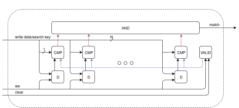
Figure 1. The structure of one line of CAM
In Fig. 1, D is a regular D-trigger for storing data; the number of these triggers in the line corresponds to the width of the input data word in CAM. VALID - D-trigger, which stores '1' if the data in the line is relevant. CMP is a comparator that compares the value of the corresponding search key bus bit if VALID = '1'. write data - write data bus, bitwise connected to the corresponding D ( N - CAM word width), we - write flag, clear - reset VALID (invalidation of the data line). AND - logical AND from N outputs of the comparators, match - flag turning into '1' if the search in this line is successful.
So, we have one line in which we can search. Now combine them:
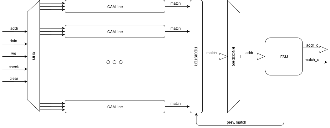
Figure 2. CAM structure
In Fig. 2, CAM_line is the actual CAM line from Fig. 1, MUX is the input address multiplexer, MATCH REGISTER is a register that stores the values of match flags, ENCODER is a decoder that converts the matches bus to the lowest match address found. FSM is a controlling finite state machine, which is prev. match removes from MATCH REGISTER the bit corresponding to the sent address so that ENCODER switches to the next found address. The interface of our CAM will be as follows:
| Line | Direction | Appointment |
|---|---|---|
| addr | entrance | Write / Erase Address |
| data | entrance | Record / Key Data |
| we | entrance | Record flag |
| check | entrance | Key Search Flag |
| clear | entrance | Flag disability line at |
| addr_o | Exit | Address found by key |
| match_o | Exit | Key Search Success Flag |
Table 1. CAM Interface
Below in Fig. 3 is a timing diagram of the operation of this interface, which shows first the recording of three words in the CAM, then a successful search, erasure and search again:
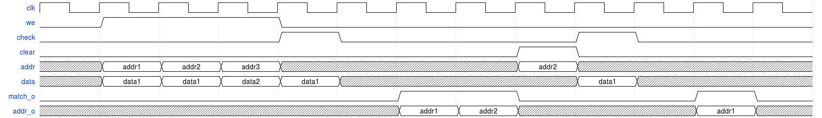
Figure 3. Timing diagram of the interface to the CAM
So, we have a description of CAM, let's move on to the synthesis.
Synthesis
We will synthesize in Xilinx ISE to compare the results with those obtained in XAPP1151 .
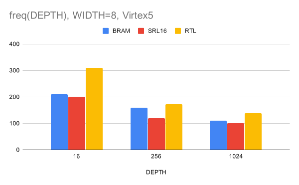
Figure 4. Frequency dependence after XST (synthesizer as part of ISE) on CAM depth for 8-bit data bus width
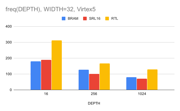
Figure 5. Frequency after XST versus CAM depth for 32-bit data bus width
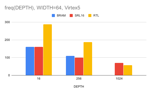
Figure 6. Frequency after XST versus CAM depth for 64-bit data bus width
In Fig. 6, there is no data for Virtex5 , since CAM of this size did not fit into the existing BRAM. We also note that for a width of 64 bits and a depth of 1024, our result was slightly worse than that of the implementation on SRL16. Now let's move on to Vivado synthesis for the XC7K325T . The results are as follows:
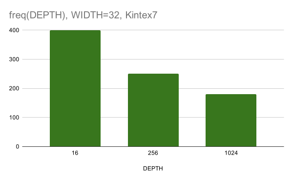
Figure 7. Frequency dependence after PnR (placement of blocks on the chip and signal tracing) on the CAM depth for a 32-bit data bus width
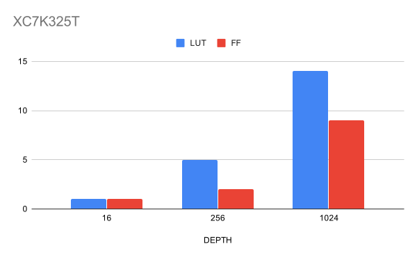
Figure 8. Utilization of resources for various CAM depths for a data width of 32 bits in%
It is important to note that the results on Vivado were obtained after PnR, which means that the design has no difficulties with tracing.
TCAM
As mentioned above, getting with this approach from CAM TCAM was not a particular problem. It is enough to add a data masking bus for data bits and distribute it bit by bit into comparators so that when comparing data with a key, they take into account its value. Such a change did not lead to a drop in frequency or a serious increase in the resources consumed, so we got TCAM for free.
findings
So, we managed to complete the task. The resulting design allows for sufficiently large CAM with a frequency above the target 125 MHz on the 7th Xilinx FPGA family. The result of the comparison with XAPP1151 was unexpected for me, I assumed that the implementation on BRAM, although it is very expensive in terms of resources, will overtake the frontal implementation in frequency. However, don’t celebrate victory so early, this document describes the Xilinx CAM IP-core, which allows, for example, to obtain CAM with a depth of 32K cells and a frequency of 155 MHz, based on BRAM. This result can probably be achieved in the variant proposed in the article, either by adding the stages of the pipeline, or by collecting large CAM from small ones, but I cannot immediately predict whether it will fit into the chip. In the future I’ll try to implement something similar on BRAM, but for now, thanks for your attention.
All Articles