Code Optimization Methods for Redd. Part 2: non-cacheable memory and parallel bus operation
In the last article, we found out that the cache is certainly a useful thing, but with regard to the controller logic it sometimes creates difficulties. In particular, it introduces unpredictability of pulse durations or other delays in the programmatic formation of time diagrams. Well, and in the "general programmatic" plan, the poor location of the function can reduce the gain from the cache to nothing, constantly provoking it to reboot from slow memory. I mentioned that 15 years ago we had to make a special preprocessor that fixed the problems that arose for the SPARC-8 processor, and promised that I would tell how easy it is to eliminate such difficulties when developing a synthesized Nios II processor recommended for use in the Redd complex. The time has come to fulfill the promise.

Today, our reference book will be the Embedded Design Handbook , or rather, its section 7.5. Using Tightly Coupled Memory with the Nios II Processor Tutorial . The section itself is colorful. Today we design processor systems for Intel FPGAs in the Platform Designer program. In the days of Altera, it was called QSys (hence the .qsys extension of the project file). But before QSsys appeared, everyone used its ancestor, SOPC Builder (in whose memory the .sopcinfo file extension was left ). So, although the document is marked with the Intel logo, but the pictures in it are screenshots from this SOPC Builder. It was clearly written more than ten years ago, and since then only terms have been corrected in it. True, the texts are quite modern, so this document is quite useful as a training manual.
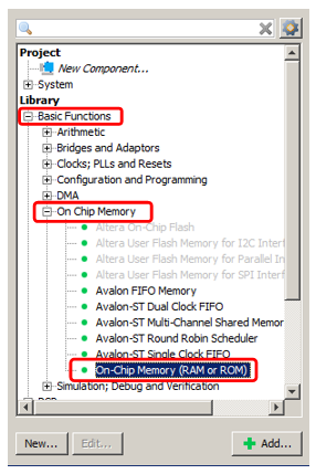
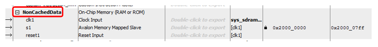
So. We want to add memory to our Spartan processor system, which is never cached and at the same time runs at the highest possible speed. Of course, this will be the internal FPGA memory. We will add memory for both code and data, but these will be different blocks. Let's start with the data memory as the simplest. We add the already known OnChip Memory to the system.
Well, let’s say its volume will be 2 kilobytes (the main problem with the FPGA’s internal memory is that it is small, so you have to save it). The rest is ordinary memory, which we have already added.

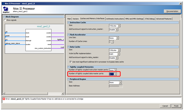
But we will not connect it to the data bus, but to a special bus. In order for it to appear, we go into the processor properties, go to the Caches and Memory Interfaces tab and in the selection list Number of tightly coulped data master ports select the value 1.
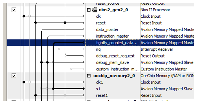
Here's a new port for the processor:

We recently connect the newly added memory block to it!
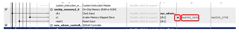
Another trick is in assigning addresses to this new memory. The document has a long line of reasoning about the optimality of address decoding. It states that non-cached memory must be distinguished from all other types of memory by a clearly expressed one bit of the address. Therefore, in the document, all non-cacheable memory belongs to the range 0x2XXXXXXX. So we enter the address 0x2000000 manually and lock it so that it does not change with the following automatic assignments.
Well, and purely for aesthetics, rename the block ... Let's call it, say, NonCachedData .
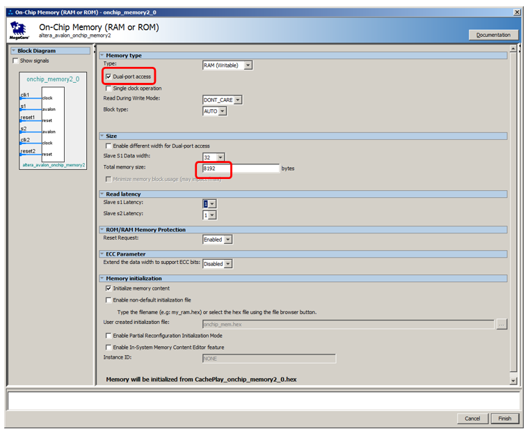
With hardware for non-cached data memory, that's it. We pass to memory for code storage. Everything is almost the same here, but a little more complicated. In fact, everything can be done completely identically, only the bus master port is opened in the Number of tightly coulped instruction master ports list, however, it will not be possible to debug such a system. When a program is filled in with the help of the debugger, it flows there through the data bus. When stopped, the disassembled code is also read by the debugger via the data bus. And even if the program is loaded from an external bootloader (we have not yet considered such a method, especially since in the free version of the development environment we are obliged to work only with the JTAG debugger connected, but in general, no one forbids doing this), the fill also goes through the bus data. Therefore, the memory will have to do dual-port. To connect to one port an uncached instruction wizard that works in the main time, and to the other - an auxiliary full-time data bus. It will be used to download the program from the outside, as well as to obtain the contents of RAM by the debugger. The rest of the time this tire will be idle. This is how it all looks in the theoretical part of the document:

Add a non-cacheable instruction port to the processor:

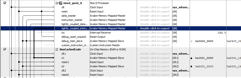
We call the memory NonCachedCode , connect the memory to the buses, assign it the address 0x20010000 and lock it (for both ports). Total, we get something like this:
All. We save and generate the system, collect the project. The hardware is ready. We pass to the software part.
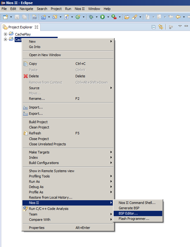
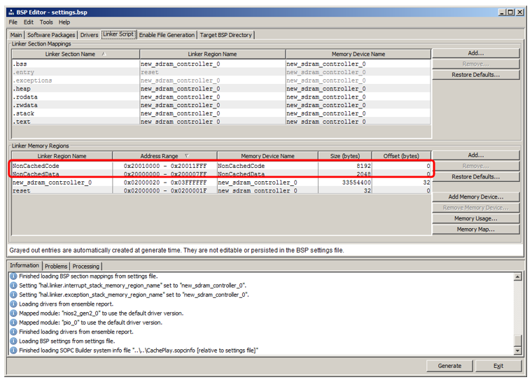
Usually, after changing the processor system, just select the Generate BSP menu item, but today we have to open the BSP Editor. Since we rarely do this, let me remind you where the corresponding menu item is located:
There we go to the Linker Script tab. We see that we have added regions that inherit names from RAM blocks:
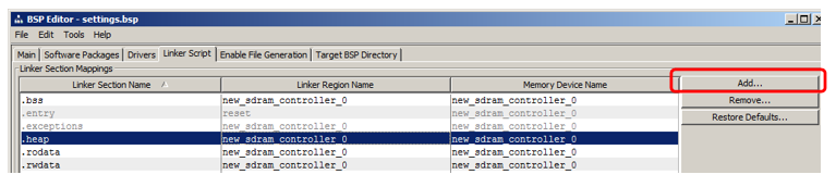
I will show how to add a section in which the code will be placed. In the section section, click Add:
In the window that appears, give the name of the section (to avoid confusion in the article, I will name it very unlike the name of the region, namely nccode) and associate it with the region (I chose NonCachedCode from the list):

That's it, generate the BSP and close the editor.
Let me remind you that we have two functions in the program inherited from the previous article: MagicFunction1 () and MagicFunction2 () . On the first pass, both of them loaded their bodies into the cache, which was visible on the oscilloscope. Further - depending on the situation in the environment, they worked either at maximum speed or constantly rubbing each other with their bodies, provoking constant downloads from SDRAM.
Let's move the first function to a new non-cached segment, and leave the second in place, and then perform a couple of runs.
We perform the first run of one iteration of the loop (I put a breakpoint on the while line):
We see the following result:
As you can see, the first function is really executed at maximum speed, the second is loaded from SDRAM. Run the second run:
Both functions operate at maximum speed. And the first function does not unload the second from the cache, despite the fact that between them is the insert that I left after writing the last article:
This insertion no longer affects the relative position of the two functions, since the first of them left in a completely different area of memory.
Similarly, you can create a section of non-cached data and place global variables there, assigning them the same attribute, but to save space, I will not give such examples.
We have created a region for such memory, mapping to the section can be done in the same way as for the code section. It remains only to understand how to assign the corresponding attribute to a variable. Here is the first example of declaring such data found in the bowels of automatically generated code:
Well, actually, from obvious things: now we can place the main part of the code in the SDRAM, and in the non-cacheable section we can put out those functions that form time diagrams programmatically, or whose performance should be maximum, which means they should not be slowed down due to that some other function constantly dumps the corresponding code from the cache.
Now take a close look at the tires in the resulting processor system. We got almost four of them. I circled red the main bus (which is the union of the two, which is why I wrote “almost”: physically - there are two tires, but logically - one). I highlighted in green the bus leading to the non-cached instruction memory, in blue - to the non-cached data memory. These three tires work in parallel and independently of each other!
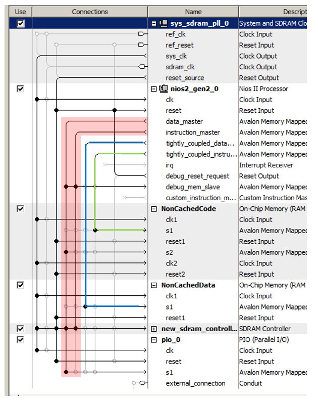
Remember, in the article about DMA, I argued that one of the performance limiting factors is that data is transmitted on the same bus? The DMA block reads data from the bus, writes data to it, and even at the same time the processor core uses the same bus. As you can see, this drawback of closed systems is completely eliminated in the FPGA. In ready-made controllers, manufacturers, when laying connections, are forced to tear between needs and capabilities. The programmer may need this option. And such. And such. And so ... A lot of things may be needed. But resources cost money, and there is not always enough space for them on the selected crystal. You can’t post everything. We have to choose what everyone really needs and what is needed in isolated cases. And which isolated cases should be introduced, and which ones should be forgotten. And then compromise solutions appear, all the subtleties of which, if there is a desire to use them, the programmer has to keep in mind. In our case, we can act without further ado. What we need today is today laid. Our resource is flexible. We spend it so that the equipment is optimal for our today's task. For tomorrow's and yesterday's tasks, resources do not need to be reserved. But under today's, we will put everything so that the program works as efficiently as possible, without requiring special programming delights.
Once upon a time, at a university in a course on signal processors we were taught the art of using two buses in parallel with one team. As far as I know, in modern ARM controllers, detailed knowledge of the bus matrix also allows optimization. But all this is good when a developer has been working with the same system for years. If you have to skip to completely different pieces of hardware from project to project, you can’t memorize everything. In the case of FPGAs, we do not study the features of the environment, we are free to customize the environment for ourselves.
We see three independent connections. Input data (in this figure it is a bus projected onto the memory), output data (in this figure it is a completely different type of bus - a stream interface) and communication with the control processor. No one bothers to connect it all to different buses, then the work will go in parallel. Input data (for example, from SDRAM) will go in one stream, which no one interferes with; the output will go in a different stream, say, to the FT245-FIFO channel, which we have already considered; and the central processor will not eat away from these clock buses, since the main bus is isolated. Although in this case, of course, the memory in SDRAM, being on a separate bus, will be programmatically unavailable. But no one will prevent it from being read by DMA. If the goal is to achieve high performance with the buffer, then it must be achieved at all costs. Unless the whole program will have to fit in the memory built into the FPGA, since there are no other storage units in the Redd hardware.
To parallelize tires, you can also use non-cached tires, because we saw that there can be several. A number of restrictions are imposed on slaves connected to these buses:
If these conditions are met, such a slave device can be connected to an uncached bus. Of course, most likely, it will be a data bus.
In general, knowing these basic principles, you can certainly use them in real tasks. But, in general, you can. You can do without this, if the result is achieved by conventional means. But keep it in mind. Sometimes, optimizing a system through these mechanisms is simpler than fine-tuning the program.
We examined a technique for transferring sections of code critical to performance or to the predictability of processing execution in non-cached memory. Along the way, we examined the possibility of optimizing performance through the use of several tires operating in parallel and independently of each other.
To finish the topic, we still have to learn how to raise the system clock frequency (now it is limited to the component generating clock pulses for the SDRAM chip). But since the articles follow the principle of “one thing - one article”, we will do it the next time.
Previous articles in the series:
- Development of the simplest “firmware” for FPGAs installed in Redd, and debugging using the memory test as an example.
- Development of the simplest “firmware” for FPGAs installed in Redd. Part 2. Program code.
- Development of its own core for embedding in a FPGA-based processor system.
- Development of programs for the central processor Redd on the example of access to the FPGA.
- The first experiments using the streaming protocol on the example of the connection of the CPU and the processor in the FPGA of the Redd complex.
- Merry Quartusel, or how the processor has come to such a life.
- Code Optimization Methods for Redd. Part 1: cache effect.
Today, our reference book will be the Embedded Design Handbook , or rather, its section 7.5. Using Tightly Coupled Memory with the Nios II Processor Tutorial . The section itself is colorful. Today we design processor systems for Intel FPGAs in the Platform Designer program. In the days of Altera, it was called QSys (hence the .qsys extension of the project file). But before QSsys appeared, everyone used its ancestor, SOPC Builder (in whose memory the .sopcinfo file extension was left ). So, although the document is marked with the Intel logo, but the pictures in it are screenshots from this SOPC Builder. It was clearly written more than ten years ago, and since then only terms have been corrected in it. True, the texts are quite modern, so this document is quite useful as a training manual.
Equipment Preparation
So. We want to add memory to our Spartan processor system, which is never cached and at the same time runs at the highest possible speed. Of course, this will be the internal FPGA memory. We will add memory for both code and data, but these will be different blocks. Let's start with the data memory as the simplest. We add the already known OnChip Memory to the system.
Well, let’s say its volume will be 2 kilobytes (the main problem with the FPGA’s internal memory is that it is small, so you have to save it). The rest is ordinary memory, which we have already added.
But we will not connect it to the data bus, but to a special bus. In order for it to appear, we go into the processor properties, go to the Caches and Memory Interfaces tab and in the selection list Number of tightly coulped data master ports select the value 1.
Here's a new port for the processor:
We recently connect the newly added memory block to it!
Another trick is in assigning addresses to this new memory. The document has a long line of reasoning about the optimality of address decoding. It states that non-cached memory must be distinguished from all other types of memory by a clearly expressed one bit of the address. Therefore, in the document, all non-cacheable memory belongs to the range 0x2XXXXXXX. So we enter the address 0x2000000 manually and lock it so that it does not change with the following automatic assignments.
Well, and purely for aesthetics, rename the block ... Let's call it, say, NonCachedData .
With hardware for non-cached data memory, that's it. We pass to memory for code storage. Everything is almost the same here, but a little more complicated. In fact, everything can be done completely identically, only the bus master port is opened in the Number of tightly coulped instruction master ports list, however, it will not be possible to debug such a system. When a program is filled in with the help of the debugger, it flows there through the data bus. When stopped, the disassembled code is also read by the debugger via the data bus. And even if the program is loaded from an external bootloader (we have not yet considered such a method, especially since in the free version of the development environment we are obliged to work only with the JTAG debugger connected, but in general, no one forbids doing this), the fill also goes through the bus data. Therefore, the memory will have to do dual-port. To connect to one port an uncached instruction wizard that works in the main time, and to the other - an auxiliary full-time data bus. It will be used to download the program from the outside, as well as to obtain the contents of RAM by the debugger. The rest of the time this tire will be idle. This is how it all looks in the theoretical part of the document:
Note that the document does not explain why, but it is noted that even with dual-port memory, only one port can be connected to an uncached master. The second should be connected to the usual.Let's add 8 kilobytes of memory, make it dual-port, leave the rest by default:
Add a non-cacheable instruction port to the processor:
We call the memory NonCachedCode , connect the memory to the buses, assign it the address 0x20010000 and lock it (for both ports). Total, we get something like this:
All. We save and generate the system, collect the project. The hardware is ready. We pass to the software part.
Preparation of BSP in the software part
Usually, after changing the processor system, just select the Generate BSP menu item, but today we have to open the BSP Editor. Since we rarely do this, let me remind you where the corresponding menu item is located:
There we go to the Linker Script tab. We see that we have added regions that inherit names from RAM blocks:
I will show how to add a section in which the code will be placed. In the section section, click Add:
In the window that appears, give the name of the section (to avoid confusion in the article, I will name it very unlike the name of the region, namely nccode) and associate it with the region (I chose NonCachedCode from the list):
That's it, generate the BSP and close the editor.
Placing code in a new memory section
Let me remind you that we have two functions in the program inherited from the previous article: MagicFunction1 () and MagicFunction2 () . On the first pass, both of them loaded their bodies into the cache, which was visible on the oscilloscope. Further - depending on the situation in the environment, they worked either at maximum speed or constantly rubbing each other with their bodies, provoking constant downloads from SDRAM.
Let's move the first function to a new non-cached segment, and leave the second in place, and then perform a couple of runs.
To place a function in a new section, add the section attribute to it.Before defining the MagicFunction1 () function, we also place its declaration with this attribute:
void MagicFunction1()__attribute__ ((section("nccode"))); void MagicFunction1() { IOWR (PIO_0_BASE,0,1); IOWR (PIO_0_BASE,0,0); ...
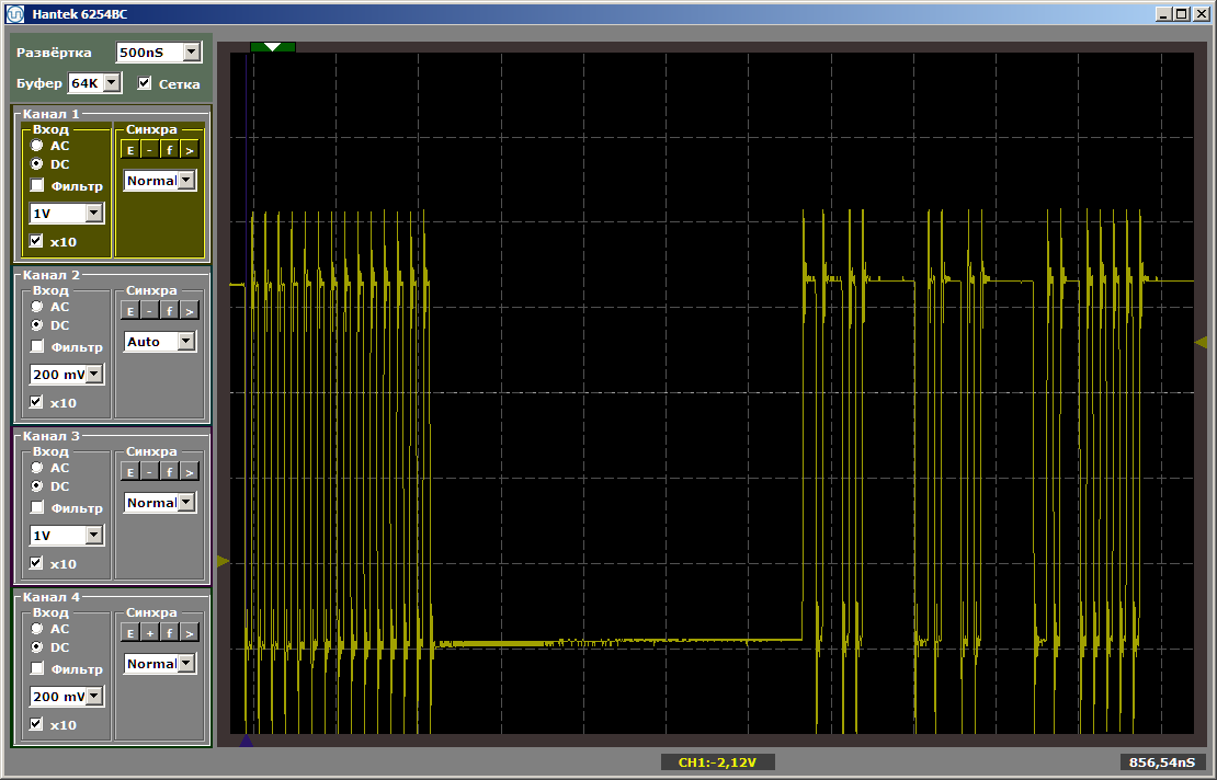
We perform the first run of one iteration of the loop (I put a breakpoint on the while line):
while (1) { MagicFunction1(); MagicFunction2(); }
We see the following result:
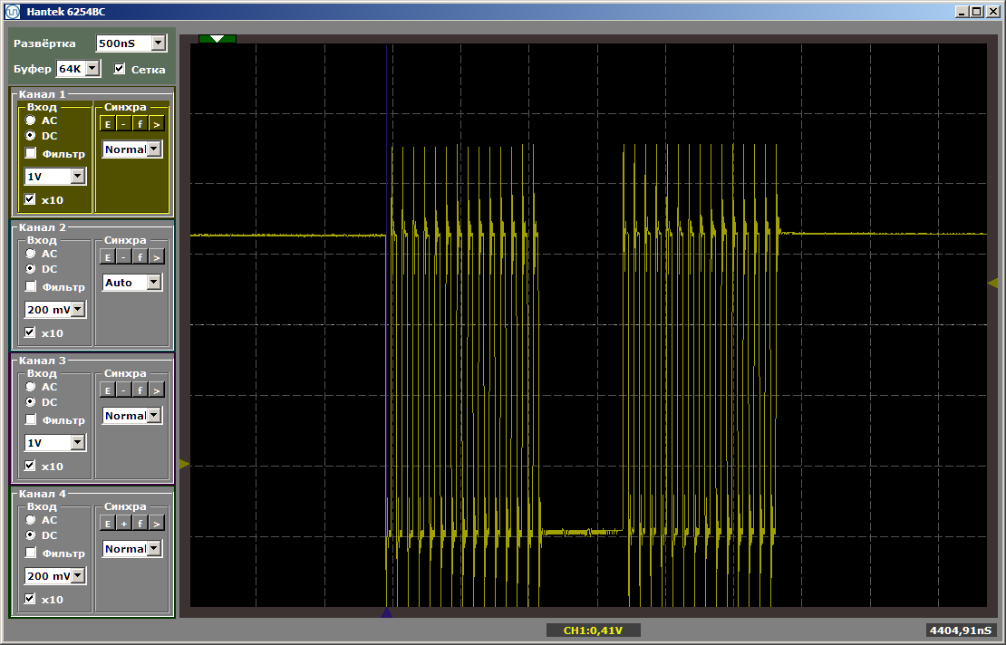
As you can see, the first function is really executed at maximum speed, the second is loaded from SDRAM. Run the second run:
Both functions operate at maximum speed. And the first function does not unload the second from the cache, despite the fact that between them is the insert that I left after writing the last article:
volatile void FuncBetween() { Nops256 Nops256 Nops256 Nops64 Nops64 Nops64 Nops16 Nops16 }
This insertion no longer affects the relative position of the two functions, since the first of them left in a completely different area of memory.
A few words about data
Similarly, you can create a section of non-cached data and place global variables there, assigning them the same attribute, but to save space, I will not give such examples.
We have created a region for such memory, mapping to the section can be done in the same way as for the code section. It remains only to understand how to assign the corresponding attribute to a variable. Here is the first example of declaring such data found in the bowels of automatically generated code:
volatile alt_u32 alt_log_boot_on_flag \ __attribute__ ((section (".sdata"))) = ALT_LOG_BOOT_ON_FLAG_SETTING;
What does it give us
Well, actually, from obvious things: now we can place the main part of the code in the SDRAM, and in the non-cacheable section we can put out those functions that form time diagrams programmatically, or whose performance should be maximum, which means they should not be slowed down due to that some other function constantly dumps the corresponding code from the cache.
Take a close look at the tires.
Now take a close look at the tires in the resulting processor system. We got almost four of them. I circled red the main bus (which is the union of the two, which is why I wrote “almost”: physically - there are two tires, but logically - one). I highlighted in green the bus leading to the non-cached instruction memory, in blue - to the non-cached data memory. These three tires work in parallel and independently of each other!
Remember, in the article about DMA, I argued that one of the performance limiting factors is that data is transmitted on the same bus? The DMA block reads data from the bus, writes data to it, and even at the same time the processor core uses the same bus. As you can see, this drawback of closed systems is completely eliminated in the FPGA. In ready-made controllers, manufacturers, when laying connections, are forced to tear between needs and capabilities. The programmer may need this option. And such. And such. And so ... A lot of things may be needed. But resources cost money, and there is not always enough space for them on the selected crystal. You can’t post everything. We have to choose what everyone really needs and what is needed in isolated cases. And which isolated cases should be introduced, and which ones should be forgotten. And then compromise solutions appear, all the subtleties of which, if there is a desire to use them, the programmer has to keep in mind. In our case, we can act without further ado. What we need today is today laid. Our resource is flexible. We spend it so that the equipment is optimal for our today's task. For tomorrow's and yesterday's tasks, resources do not need to be reserved. But under today's, we will put everything so that the program works as efficiently as possible, without requiring special programming delights.
Once upon a time, at a university in a course on signal processors we were taught the art of using two buses in parallel with one team. As far as I know, in modern ARM controllers, detailed knowledge of the bus matrix also allows optimization. But all this is good when a developer has been working with the same system for years. If you have to skip to completely different pieces of hardware from project to project, you can’t memorize everything. In the case of FPGAs, we do not study the features of the environment, we are free to customize the environment for ourselves.
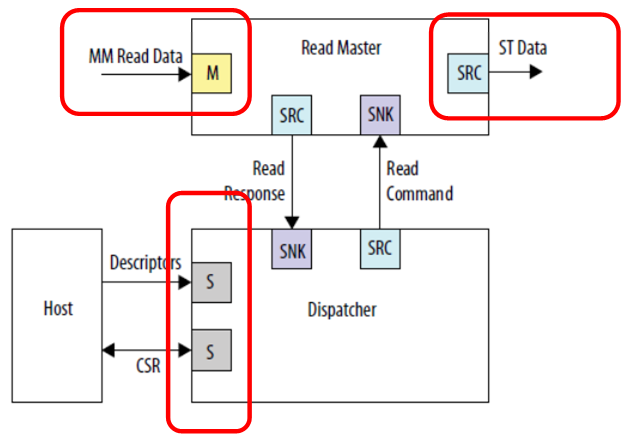
In relation to the approach “we do not spend much time on development”, it sounds like this:Let's take a look at an example of including a DMA block from the Embedded Peripherals IP User Guide to consolidate the material.
We do not need to make efforts to optimize the use of ready-made standard tires, we can quickly lay them in the most optimal way for the task to be solved, quickly finish this auxiliary development and quickly ensure the process of debugging or testing the main project.
We see three independent connections. Input data (in this figure it is a bus projected onto the memory), output data (in this figure it is a completely different type of bus - a stream interface) and communication with the control processor. No one bothers to connect it all to different buses, then the work will go in parallel. Input data (for example, from SDRAM) will go in one stream, which no one interferes with; the output will go in a different stream, say, to the FT245-FIFO channel, which we have already considered; and the central processor will not eat away from these clock buses, since the main bus is isolated. Although in this case, of course, the memory in SDRAM, being on a separate bus, will be programmatically unavailable. But no one will prevent it from being read by DMA. If the goal is to achieve high performance with the buffer, then it must be achieved at all costs. Unless the whole program will have to fit in the memory built into the FPGA, since there are no other storage units in the Redd hardware.
To parallelize tires, you can also use non-cached tires, because we saw that there can be several. A number of restrictions are imposed on slaves connected to these buses:
- the slave is always one on the bus;
- the slave does not use the bus delay mechanism;
- write latency is always zero; read latency is always one.
If these conditions are met, such a slave device can be connected to an uncached bus. Of course, most likely, it will be a data bus.
In general, knowing these basic principles, you can certainly use them in real tasks. But, in general, you can. You can do without this, if the result is achieved by conventional means. But keep it in mind. Sometimes, optimizing a system through these mechanisms is simpler than fine-tuning the program.
Conclusion
We examined a technique for transferring sections of code critical to performance or to the predictability of processing execution in non-cached memory. Along the way, we examined the possibility of optimizing performance through the use of several tires operating in parallel and independently of each other.
To finish the topic, we still have to learn how to raise the system clock frequency (now it is limited to the component generating clock pulses for the SDRAM chip). But since the articles follow the principle of “one thing - one article”, we will do it the next time.
All Articles