History of the Ethernet-CAN Converter
One clear sunny day for work needed an inexpensive CAN to Ethernet interface converter. Naturally, the search began with ready-made solutions, but, as often happens, in the end it was decided to develop their own sample. Naturally, the author’s enthusiasm could not resist and limited himself to such a “truncated” functionality. What came of it, how and why - under the cut.
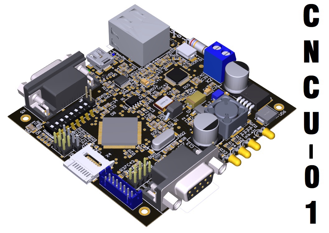
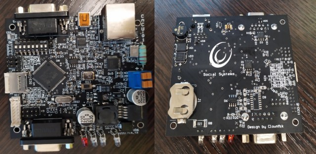
General summary. The photo above shows a 3D model of the board I developed using CAD Altium Designer. Key features and functionality:
The cost of the collected board is ~ 5000 R. The project is open source in nature, the sources can be found on github . What turned out as a result, in addition to the main functionality, can be considered a good debugging board for working with the STM32 microcontroller.
And now to the details of the creation.
The study of this problem began with the search and evaluation of ready-made solutions. The main requirements were:
Colleagues from China have several industrial solutions, but not cheap ones, so a representative of the domestic production PIRS CAN-Ethernet Interface Converter was delivered to our office for a test. According to the described capabilities and characteristics, the device satisfied the modest T.Z., it only remained to check the performance in practice, which I did, armed with Wireshark and the oscilloscope. For some unknown reason, when sending packets to the TCP device at the device’s output, where the CAN frames were supposed to appear, sequences with physical CAN levels (differential pair) but logical UART interface protocol (with start and stop bits) spit out. Opening the case, opening the documentation of the microcircuits and ringing the board tracks, I found that, indeed, the RX and TX (UART) pins of the microcontroller are connected to the CAN transceiver and are connected to an external connector from it. Thus, no hardware support for the CAN2.0B standard was to be expected.
Here is what I saw on the CANL output of “PIRS CAN-Ethernet” when sending two bytes of data [ 0xF0 ] and [ 0x0A ] over TCP \ IP:
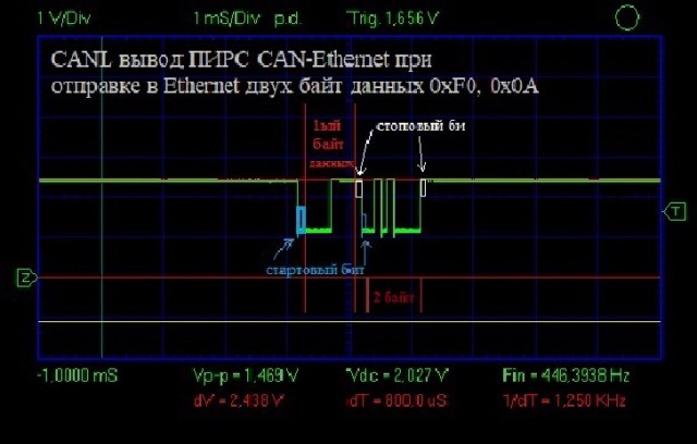
The order of the bits is turned upside down, but you can deal with it programmatically, but it is already more difficult to do something at the application level with start and stop bits through each byte, because they are inserted in hardware.
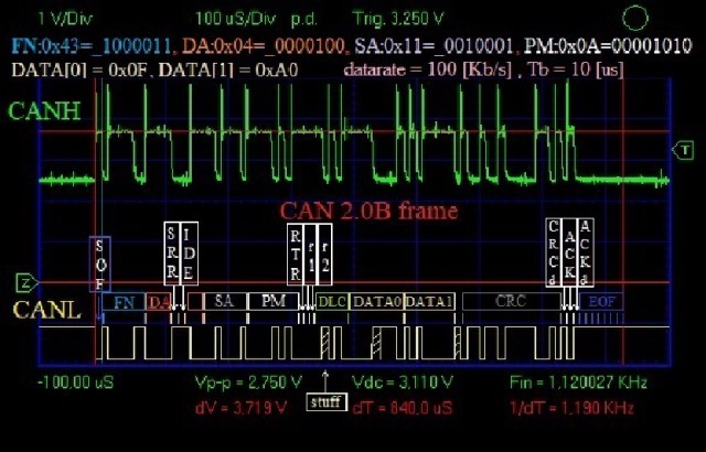
And here is what the “true” CAN2.0B frame with the same two bytes of data should look like:

As you can see from the waveform, in addition to data bytes, the frame contains many service bits of the protocol plus stuffing bits, and most importantly, they go continuously without any start and stop bits! (For those who are interested, under the spoiler a detailed description of this package).
Thus, it was not possible for me to solve the problem of inconsistency between CAN and UART frames programmatically, and, looking at the intermediate research results with a disappointed look, it was decided to develop our own prototype of the required device.
Due to the fact that now it was possible to take control of a wider range of technical characteristics of the device, the following requirements were added:
3. The ability to power from 12-24 V in transport systems;
4. The presence of external memory for storing logs;
5. The dimensions of the board are not more than 86x80mm.
6. Operating temperature range -40..85 ° C
The notorious STM32F407VET6 platform [2] was chosen as the brain of the new device, which has hardware support for all the necessary interfaces and a good supply of RAM and FLASH memory. Having polished the Internet, the DP83848IVV transceiver [3] was selected as PHY Ethernet, which has, in my opinion, good documentation and enough examples of schemes with connection and tracing. As an external non-volatile memory for storing logs, I chose SPI FLASH 2 MB and SPI EEPROM for storing various settings. In addition, power protection against overvoltage, polarity reversal was added. After N evenings and M weekends, a circuit diagram and a trace of the printed circuit board of the device of the first version were compiled. Because there was enough space on the board, but I did not want to leave the unused MK legs, in addition to the main functionality, the board was added:
The idea was that, if necessary, the board was ready to expand the functionality by installing additional components. Moreover, spare seats do not affect the cost of production. On one side, unfortunately, because of this, it was not possible to fit everything, so the board turned out to be bilateral 86x80mm, min. track width 0.25mm, min hole diameter 0.6mm.
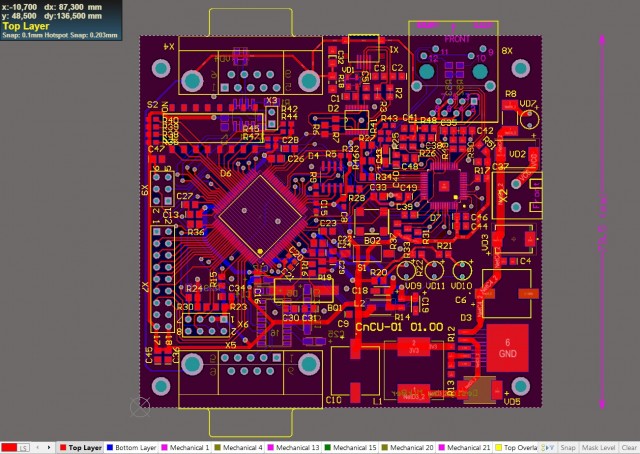
The first version of PCB design
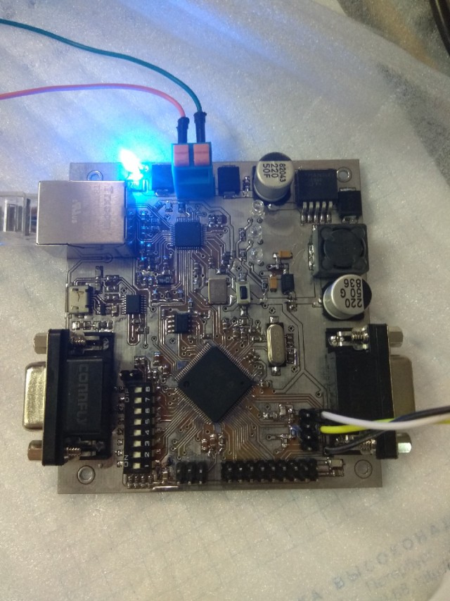
Later, two test samples were ordered and assembled with a complete set of peripherals for research. In order to save money, the board was made without a mask and therefore has such an uncharacteristic color.
Using STM32CubeMX, I sketched a test firmware with a test of the main peripheral modules of the device and, to a first approximation, everything worked, except for starting the MC from an external 8 MHz quartz. It turned out, due to my mistake in drawing up the specification, the wrong load capacitors were soldered. But this did not stop the STM32F407 from working with an internal RC generator. When I was able to ping my device, there was no restraining joy. I’ve probably taken the longest with PHY Ethernet tracing. Then in the browser I saw my test http page and calmed down with testing.
The production of the first samples of the boards was ordered in Zelenograd. And, despite the fact that the cost of “with” the mask and “without” was almost two times different, I do not recommend doing it even at the prototype stage, because, as a rule, it is at this stage that the tracing errors pop up and something solder. But to get drunk on the “bare” tracks is extremely unpleasant, save money, but hardly any nerves. Yes, and guessing then whether it shortened somewhere or the trace is incorrect is such a pleasure. Due to my inexperience, soldering a quartz resonator and load capacitors, I killed one sample.
By that time, at work, in the bins there was a piece of iron capable of solving the conversion task in the current project, but, in addition to the large size and cost, having started writing firmware for it, I ran into problems related to the RAM size and the truncated TCP \ IP functionality of the MK stack LPC2368. So the desire to make your device only intensified.
Having carefully studied the shortcomings of the first version, I, without thinking twice, proceeded to the second. And again I wanted to add a “backlog for the future”, incorporating the following components into the previous form factor:
Among other things, current power protection and TVS diodes on user connectors were added.
The result is a kind of dev-board with the ability to connect external modules. This time I ordered a board in China. The assembly was carried out with us.

The second version of the board
For the second version, I figured out 3D modeling in Altium Designer, which helped a lot to avoid errors in the relative positioning of components on two sides (it turned out that the Internet already had a lot of ready-made models of SMD components [4] ). Thus, all the errors of the first version were fixed, the innovations showed their efficiency, which made me very happy.
The description of the code is beyond the scope of this part, however I would like to say a few words about the software component. In my device, I decided to use the FreeRTOS + LwIP stack. There are a sufficient number of articles about them, for example, [5] and [6] , so it should not be difficult to tie them to your project. In short, LwIP is a TCP \ IP stack for embedded systems, characterized by low RAM consumption and a convenient API (there is even a BCD socket shell). I used the netconn API. By means of FreeRTOS, all the work of the TCP \ IP stack is placed in a stream separate from the application. In addition to the main work (connecting an external TCP server to the CAN bus), a separate web server is spinning in an independent stream to access the device settings. Such a web interface is intended for monitoring and configuration of device settings - setting different operating modes, transmission speeds, addresses, etc. I do not know yet whether it will be possible to make a firmware update through it.
This was my first (and I hope not the last) hardware project of such complexity and, despite the mistakes made, the second version of the board, I think, can be considered successful. At each iteration, there were many doubts, but, nevertheless, I am convinced once again that if you do not try, nothing will surely turn out.
1. Wikipedia / Controller_Area_Network
2. STM32F407VET6 datasheet
3. DP83848 datasheet
4. 3D Models
5. Introduction to FreeRTOS
6. Introduction to LwIP
General summary. The photo above shows a 3D model of the board I developed using CAD Altium Designer. Key features and functionality:
- 10 \ 100 Mb Ethernet
- Rtc
- MicroSD (FAT12, FAT16, FAT32) 4GB
- RS232 \ RS485
- CAN
- Buzzer
- 3 User LED
- GPIO
- EEPROM 32 KB
- FLASH 2 MB
- I2C
- SPI
- UART
- SW \ JTAG
- USB serial (COM Port)
- Power: miniUSB 5V \ External 9..24V
The cost of the collected board is ~ 5000 R. The project is open source in nature, the sources can be found on github . What turned out as a result, in addition to the main functionality, can be considered a good debugging board for working with the STM32 microcontroller.
And now to the details of the creation.
Hardware
The study of this problem began with the search and evaluation of ready-made solutions. The main requirements were:
- conversion of incoming CAN2.0B frames to TCP \ IP packets and vice versa;
- low cost, as a result, the implementation of a device based on a microcontroller.
Colleagues from China have several industrial solutions, but not cheap ones, so a representative of the domestic production PIRS CAN-Ethernet Interface Converter was delivered to our office for a test. According to the described capabilities and characteristics, the device satisfied the modest T.Z., it only remained to check the performance in practice, which I did, armed with Wireshark and the oscilloscope. For some unknown reason, when sending packets to the TCP device at the device’s output, where the CAN frames were supposed to appear, sequences with physical CAN levels (differential pair) but logical UART interface protocol (with start and stop bits) spit out. Opening the case, opening the documentation of the microcircuits and ringing the board tracks, I found that, indeed, the RX and TX (UART) pins of the microcontroller are connected to the CAN transceiver and are connected to an external connector from it. Thus, no hardware support for the CAN2.0B standard was to be expected.
Here is what I saw on the CANL output of “PIRS CAN-Ethernet” when sending two bytes of data [ 0xF0 ] and [ 0x0A ] over TCP \ IP:
The order of the bits is turned upside down, but you can deal with it programmatically, but it is already more difficult to do something at the application level with start and stop bits through each byte, because they are inserted in hardware.
And here is what the “true” CAN2.0B frame with the same two bytes of data should look like:
As you can see from the waveform, in addition to data bytes, the frame contains many service bits of the protocol plus stuffing bits, and most importantly, they go continuously without any start and stop bits! (For those who are interested, under the spoiler a detailed description of this package).
Spoiler
Thus, it was not possible for me to solve the problem of inconsistency between CAN and UART frames programmatically, and, looking at the intermediate research results with a disappointed look, it was decided to develop our own prototype of the required device.
Due to the fact that now it was possible to take control of a wider range of technical characteristics of the device, the following requirements were added:
3. The ability to power from 12-24 V in transport systems;
4. The presence of external memory for storing logs;
5. The dimensions of the board are not more than 86x80mm.
6. Operating temperature range -40..85 ° C
The notorious STM32F407VET6 platform [2] was chosen as the brain of the new device, which has hardware support for all the necessary interfaces and a good supply of RAM and FLASH memory. Having polished the Internet, the DP83848IVV transceiver [3] was selected as PHY Ethernet, which has, in my opinion, good documentation and enough examples of schemes with connection and tracing. As an external non-volatile memory for storing logs, I chose SPI FLASH 2 MB and SPI EEPROM for storing various settings. In addition, power protection against overvoltage, polarity reversal was added. After N evenings and M weekends, a circuit diagram and a trace of the printed circuit board of the device of the first version were compiled. Because there was enough space on the board, but I did not want to leave the unused MK legs, in addition to the main functionality, the board was added:
- debugging tools SW, JTAG;
- 8-DIP Switch;
- micro-USB (USB Serial);
- RS-232;
- UART
- I2C;
- GPIO
The idea was that, if necessary, the board was ready to expand the functionality by installing additional components. Moreover, spare seats do not affect the cost of production. On one side, unfortunately, because of this, it was not possible to fit everything, so the board turned out to be bilateral 86x80mm, min. track width 0.25mm, min hole diameter 0.6mm.
The first version of PCB design
Later, two test samples were ordered and assembled with a complete set of peripherals for research. In order to save money, the board was made without a mask and therefore has such an uncharacteristic color.
Using STM32CubeMX, I sketched a test firmware with a test of the main peripheral modules of the device and, to a first approximation, everything worked, except for starting the MC from an external 8 MHz quartz. It turned out, due to my mistake in drawing up the specification, the wrong load capacitors were soldered. But this did not stop the STM32F407 from working with an internal RC generator. When I was able to ping my device, there was no restraining joy. I’ve probably taken the longest with PHY Ethernet tracing. Then in the browser I saw my test http page and calmed down with testing.
The production of the first samples of the boards was ordered in Zelenograd. And, despite the fact that the cost of “with” the mask and “without” was almost two times different, I do not recommend doing it even at the prototype stage, because, as a rule, it is at this stage that the tracing errors pop up and something solder. But to get drunk on the “bare” tracks is extremely unpleasant, save money, but hardly any nerves. Yes, and guessing then whether it shortened somewhere or the trace is incorrect is such a pleasure. Due to my inexperience, soldering a quartz resonator and load capacitors, I killed one sample.
By that time, at work, in the bins there was a piece of iron capable of solving the conversion task in the current project, but, in addition to the large size and cost, having started writing firmware for it, I ran into problems related to the RAM size and the truncated TCP \ IP functionality of the MK stack LPC2368. So the desire to make your device only intensified.
Having carefully studied the shortcomings of the first version, I, without thinking twice, proceeded to the second. And again I wanted to add a “backlog for the future”, incorporating the following components into the previous form factor:
- RTC support with battery;
- RS-485;
- micro-SD;
- buzzer tweeter;
- the ability to power from USB;
- SPI to external connector;
- 5V and 3.3V power to an external connector.
Among other things, current power protection and TVS diodes on user connectors were added.
The result is a kind of dev-board with the ability to connect external modules. This time I ordered a board in China. The assembly was carried out with us.
The second version of the board
For the second version, I figured out 3D modeling in Altium Designer, which helped a lot to avoid errors in the relative positioning of components on two sides (it turned out that the Internet already had a lot of ready-made models of SMD components [4] ). Thus, all the errors of the first version were fixed, the innovations showed their efficiency, which made me very happy.
Firmware
The description of the code is beyond the scope of this part, however I would like to say a few words about the software component. In my device, I decided to use the FreeRTOS + LwIP stack. There are a sufficient number of articles about them, for example, [5] and [6] , so it should not be difficult to tie them to your project. In short, LwIP is a TCP \ IP stack for embedded systems, characterized by low RAM consumption and a convenient API (there is even a BCD socket shell). I used the netconn API. By means of FreeRTOS, all the work of the TCP \ IP stack is placed in a stream separate from the application. In addition to the main work (connecting an external TCP server to the CAN bus), a separate web server is spinning in an independent stream to access the device settings. Such a web interface is intended for monitoring and configuration of device settings - setting different operating modes, transmission speeds, addresses, etc. I do not know yet whether it will be possible to make a firmware update through it.
Conclusion
This was my first (and I hope not the last) hardware project of such complexity and, despite the mistakes made, the second version of the board, I think, can be considered successful. At each iteration, there were many doubts, but, nevertheless, I am convinced once again that if you do not try, nothing will surely turn out.
Sources used
1. Wikipedia / Controller_Area_Network
2. STM32F407VET6 datasheet
3. DP83848 datasheet
4. 3D Models
5. Introduction to FreeRTOS
6. Introduction to LwIP
All Articles