How we developed a platform for electronic jewelry
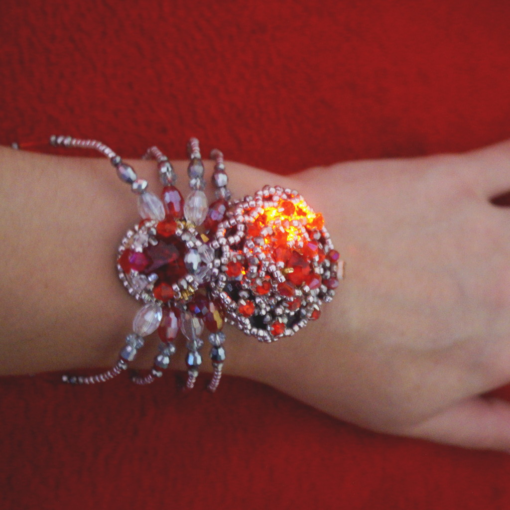
The idea to cross electronics and jewelry is very old. So when we remembered it, the search gave a large amount of work on this subject. True, often, electronic jewelery was meant as jewelery from electronics — board pieces dressed in epoxy, elements, and microchip pendants. We wanted to make LED decorations. Not the same as in Chinese toys that sell at every corner, because everything is rather uninteresting in them - there are several blinking programs that are switched by a button, but something more complicated and more interesting. For example, running lights that react to ambient lighting, burning brighter in the dark and dim in the light. Or flickering to the beat of the surrounding music. Or changing color depending on the temperature around. Or showing the heart rate of the carrier. In other words, we wanted some kind of active reaction. Immediately I say - it turned out something like this:
Warning: this article was written primarily for non-technical professionals, so it has some simplifications that may cause engineers to disapprove. Feel free to express them.
Thus, the requirements for the electronic part:
Having fixed these requirements, we began to think seriously. Like any technical problem, this one had a lot of solutions.
For example, we could take the standard constructor of the type LiliPad or Adafruit GEMMA , created just for this purpose. If you look at examples of GEMMA, then there you can see a large number of similar projects with LEDs, there are even earrings. Unfortunately, the designer is very well suited at the prototype stage, when the device needs to be assembled from dirt and sticks to check whether it works at all, but, alas, it is absolutely not suitable for any small series - interfere with additional connectors, connections and the whole construct . Well, the cost of the designer and parts to it (and we remember that we also need LEDs and sensors) also plays unpleasantly on the cost of the final product not in the direction most interesting for the buyer. So designers are a good option, but generating a large number of questions.
The alternative is to develop the electronic part entirely and independently. This way is both simpler (since we can leave only what we need) and difficult (because the creation of a programmable device even for our seemingly simple task carries a lot of pitfalls and compromise solutions). Of course, seeing such a wonderful opportunity to deflate some parts of the body, we could not pass by.
Here, probably, it is worth making a small excursion into the manufacture of electronics and how it happens.
So, we have an idea and requirements. It remains to embody them "in the gland."
Reflections on the question raised a large number of doubts:
So, we dig in the search, sort through the combinations and as a result we get the following solution that satisfies us:
Once we have decided on the components, download the documentation for the controller and the LEDs and dive into the study. The nuances come up - the LEDs are connected in series, “train” and are controlled by one wire, to which the controller must form a special signal, roughly speaking - to send a specific sequence of numbers, each of which will mean with what intensity to light each of the built-in LEDs (and we remember that in one case we have three of them - red, green and blue). Those. we need to consistently send the brightness of red, green and blue for the first LED, then for the second, then for the third and so on, depending on how many of them we have on in series. If you have seen LED tapes in building stores, iridescent with all the rays of the rainbow, then know that they work along the same lines.
In addition to controlling these LEDs, noise protection is required, which will require one capacitor per LED. In addition, the same interference capacitor is required for the microcontroller.
Further, the LEDs, even in such a compact version, are still greedy for power. Therefore, their greed should be limited, and we have one limiter - resistance. Those. Each LED requires an additional current-limiting resistor. It's funny that in the development process of the product it turned out that these resistors do not help much or how much damage - when there are more than four LEDs, there is a shortage of current and I had to change them to zero ohms, i.e. banal jumpers to LEDs work correctly. In subsequent versions of the scheme, we completely removed them.
The photoresistor also required an additional resistor playing the role of a voltage divider. Examples of schemes for connection can be found fully, if you type in a search engine “arduino photoresistor connection”.
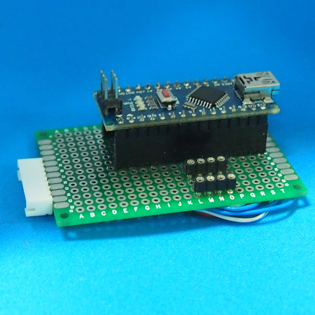
Separately, it is worth mentioning the programming of the microcontroller - in order to fill in the firmware (program code in binary form) in Attiny85, a special device is required - the “programmer”. Fortunately, it is assembled on the basis of the Arduino electronic designer (in which his elder brother is also Atmel's microcontroller, but more seriously), which can be bought at any electronic store or in China for little money.
And finally, the switch - we do not want the user to constantly insert and remove the battery.
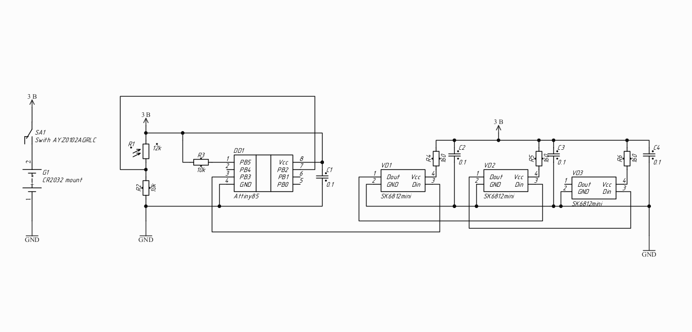
However, despite all of the above, the basic scheme turned out to be simple compared to most household appliances (most likely, your thermal lot is more complicated in electronics than our circuit):
As a result, we got a device that measures slightly larger than a conventional button-type battery. Actually the battery and the switch are placed on one side, the LEDs, the microcontroller and the light sensor on the other. Since LEDs can also affect the light sensor located nearby (let's say, light it up so that it will assume that the circle is light, although in fact there may still be darkness), it was decided to mount it with the ability to bend in a plane perpendicular to the direction glow.
As a result of the layout, we have a fairly simple printed circuit board. Before routing, we checked the circuit and it turned out to be efficient, though with one reservation - we checked it on a constant power source, and not on a battery, therefore fears that such a small battery would not last long enough until we soldered the first devices.
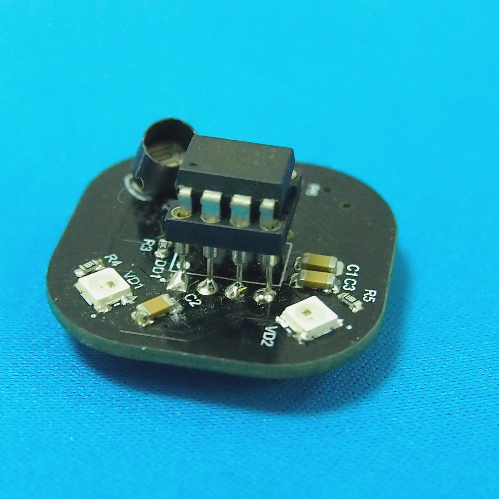
So, the scheme is done, the board is divorced. And then the first compromise is that Attiny85 microcontrollers are available in two types of enclosures - DIP (these are classic microcircuits with pin legs, which you probably saw at the dawn of electronic distribution and simple devices) and SO (these are planar microcircuits, small and compact, do not require additional holes for soldering and mounted on top of the board by soldering). At the time of designing, our supplier had a more expensive SO-version component and, most importantly, it was not available. Therefore, we took the DIP version, but with the expectation that we will first program it, and then carefully bite off the legs and solder it as SO, directly to the board. This made an additional technological risk - to change the firmware in this version after soldering the microcontroller to the board would not be a very trivial task, but who among us does not like difficulties ?!
We ordered the boards in China, this process is fine-tuned there, and we started collecting components. Light-emitting diodes and battery holders were also ordered in China, they either did not exist on the local market, or they were worth indecent money. The rest is bought in the nearest electronic supermarket. Microcontrollers could also be ordered in China, but a large number of negative responses and our own sad experience (when the components sent out did not provide enough good quality) kept us from taking this step. Therefore, by the time we received the finished printed circuit boards, the entire BoM was in our hands. There is even time left to slowly solder the programmer for microcontrollers.
After receiving the boards, we soldered one test device. Since the program for the microcontroller was postponed until the finished device was obtained (and it was right, I will tell you a little later), we did not solder the microcontroller “for good”, but made a transitional platform into which the chip can be plugged in like a light bulb into a cartridge. As expected, the device did not work. Looking closely at the device (for a couple of hours), we found an error - the LEDs were soldered incorrectly. The fact is that when mounting chips and elements with a large number of legs, it is very important not to confuse these legs and put the element correctly. To do this, the engineers on the markings on the printed circuit board use a key - an image of a point, which must coincide with the same one on the body of the chip. As a result, the process of soldering such an element looks like this - we combine the keys, solder one leg, solder all the others. To confuse the key is usually fraught with negative consequences - the author of these lines somehow shoved the microcontroller into the programmer from the wrong side - after five seconds the air smelled fried, and the finger that touched the chip got a neat burn according to the shape of the case. Fortunately, no one was hurt anymore and after cooling the microcontroller also remained working.
So, in the design of our board, we applied a self-made description for LEDs (three-millimeter SK6812s are rarely found than WS2812) and they safely made a mistake with the key. As a result, when mounting the LED key must be located on the other side relative to the key marked on the board. The test board went safely to the scrap.
The second test sample was already assembled with this error. Now we were sure that our scheme was operational and began to program the firmware.
It looked like this:
I note that sometimes during the day this operation had to be repeated several dozen times. It was possible to solder the programmer directly to the chip on the board, but, as you remember, we are not looking for easy ways.
At the programming stage, too many interesting things came to light.
It all started with the fact that none of the standard libraries work with managed LEDs did not work. The reason was not in one place, but in two. Firstly, the time intervals for coding control signals were intended for other types of LEDs and did not coincide with the ones indicated in our documentation. Secondly, in the case of battery power, the microcontroller turns out to operate at a lower frequency and, by default, can reduce it even more to save energy (which it does when the battery is used), which again leads to a change in the time intervals for controlling the LEDs. A pair of clocks with an oscilloscope helped adjust the library to the required intervals, and half an hour and a few experiments allowed us to find a command that prohibits the microcontroller from changing the frequency of operation. As a result of a mid-term battle, we were able to manage the LEDs normally, lighting them with those colors that we needed, and not in a completely random order.
The second surprise was the light sensor. After programming it, we couldn’t understand for a long time why there was no reaction to closing it with a finger (i.e., completely darkening) from the word “absolutely”. The answer came after a few days of intently peering at examples of working with such sensors. It turned out that when setting up the analog port to which the sensor was to be connected, it was necessary to use one numbering, and when reading readings, another one (yes, I also remembered the anecdote “Wow, an error in one digit, and what a difference!”) . After this realization, everything worked as it should. The firmware has been written.
Since we were sent not one, and not two printed circuit boards, but ten at once (one, as we remember, was disposed of), we soldered all the others to the joy.
It turned out that the law of large numbers also works on small lots - two out of ten boards showed a manufacturing defect - our Chinese colleagues did not have a good electrical connection between the front and back layers of the board, as a result, nothing worked due to lack of power. Fortunately, this is easily eliminated by soldering the vias with the conductor.
The devices are assembled, tested and transferred for further processing to give the appearance of the finished decoration. In fact, we spent no more than a week on the whole development, but due to distractions to other tasks and expectations (free time, components, printed circuit boards) the whole process was spread over a half-year time interval.
If anyone is interested, the source code and project materials are laid out on Github .
The story does not end there. After the first instructive experience, we made several versions of the board.
The second version was in two versions - with six LEDs in a circle and four (one in the center) and it was different in that here we used the SO-package of the chip. But even there it was not without excesses - when wiring the board because of the confusion in the names, the wrong contact area was chosen and as a result, the mounting feet of the chip had to be pressed under the case. In addition, they brought out the contacts for the firmware and the three "power-signal-ground" on separate platforms, in order to be able to add more LEDs as a remote element.
In addition, another unpleasant flaw was revealed - the master very much requested to make the board perfectly round (in our version it looked more like a rectangle with rounded corners). They did it, at the same time checking the Chinese industry on the production of boards thinner than a millimeter in thickness. The result was completely satisfactory - replacing the holders with those designed for CR2016 batteries, we got an even more lightweight platform from which you can already make, for example, earrings.
For the firmware of these devices, a programmer a la “collective farm” was used on pogo pins. As it turned out, the firmware download procedure was still non-trivial - you had to press the board tightly enough to the pins, which was not immediately possible the first time.
The apotheosis of the development of this branch of the platform was the third and latest version. In it, the contacts for the firmware were brought to a separate flexible cable, an additional fee was ordered for the programmer. At this iteration, we appreciated Seeedstudio's PCBA service, which made printed circuit boards for us — the Chinese industry brought the boards with most of the elements mounted, we soldered the connector for the programmer, the battery holder, the photoresistor and the LEDs - they were not (except for the photoresistor) components available for installation.
The result looks like this:
In general, the project turned out to be interesting. As it turned out, even seemingly simple things can conceal very complicated nuances inside, which was clearly shown.
Warning: this article was written primarily for non-technical professionals, so it has some simplifications that may cause engineers to disapprove. Feel free to express them.
Thus, the requirements for the electronic part:
- there should be several controlled LEDs (managed - this means that we can not just turn on and off their glow, but also control their brightness and, importantly, color);
- You must have at least one sensor - a light sensor, a temperature sensor, or a microphone. Pulse sensors have been set aside so far - they require a direct approach to the body (therefore, your fitness bracelet is useless in this regard if you wear it over a shirt);
- control must be programmable. This means that at any moment we can change the logic of controlling the LEDs to a more appropriate one for the surroundings of the finished decoration, for example, if cold colors prevail in the decoration, then make the glow appropriate;
- the device should be compact and light, because heavy pieces severely limit the possibility of their use;
- the circuit should be powered from batteries or from batteries that can be bought at any corner for the convenience of the consumer.
Having fixed these requirements, we began to think seriously. Like any technical problem, this one had a lot of solutions.
For example, we could take the standard constructor of the type LiliPad or Adafruit GEMMA , created just for this purpose. If you look at examples of GEMMA, then there you can see a large number of similar projects with LEDs, there are even earrings. Unfortunately, the designer is very well suited at the prototype stage, when the device needs to be assembled from dirt and sticks to check whether it works at all, but, alas, it is absolutely not suitable for any small series - interfere with additional connectors, connections and the whole construct . Well, the cost of the designer and parts to it (and we remember that we also need LEDs and sensors) also plays unpleasantly on the cost of the final product not in the direction most interesting for the buyer. So designers are a good option, but generating a large number of questions.
The alternative is to develop the electronic part entirely and independently. This way is both simpler (since we can leave only what we need) and difficult (because the creation of a programmable device even for our seemingly simple task carries a lot of pitfalls and compromise solutions). Of course, seeing such a wonderful opportunity to deflate some parts of the body, we could not pass by.
Here, probably, it is worth making a small excursion into the manufacture of electronics and how it happens.
How electronics is made on the fingers
First, the idea and requirements for the device are formed (well, what we have already done). Then these requirements are discussed with experts in electronics and jointly refined - the project is cluttered with details and nuances.
Draws a schematic diagram of the device - how electronic components must be connected to each other in order to work together. The scheme is tested in practice - from the improvised means and the first device is assembled on the wiring. If it works, it means that the initial scheme was correct and you can move on.
After we have a proven circuit diagram of the device, the most interesting part begins - PCB layout, i.e. such a piece of PCB with tracks, on which electronic components are soldered. You can, of course, do everything on the wiring, but it will be slow, boring and extremely unreliable. In addition, modern technologies have reached such a spread that it is possible to make a printed circuit board with industrial quality for very little money. However, we'll see it again. The design of the PCB is to show how we will arrange the elements and how they will be interconnected. Or, more simply, we need to redraw the concept diagram beautifully and taking into account the real physical dimensions of the parts.
Just to design a printed circuit board (“dissolve” in professional jargon) is not enough, we still need to prepare it for production, i.e. to form the correct set of documents, which includes the appearance of the result, the pattern of conductive tracks, the drilling and metallization scheme. Usually, even experienced engineers do this not immediately, especially in the case when the device is not simple. These files (in Gerber format) are transferred to production. While the printed circuit board is produced, there is a purchase of elements that will be soldered onto it. In professional language, the list of such elements is called BoM (from English Bill of Materials - the list of components).
After receiving the printed circuit board and purchasing all the necessary components, elements are mounted on the board, which can be manual (usually used for small runs up to a thousand copies) or automatic (by special machines for large batches). Manual installation looks like an engineer with a soldering iron, which simply solders the elements onto the board according to the scheme provided to it.
After the installation is completed, the device is programmed (if it contains chips that allow it) and is tested, i.e. its working capacity and resistance to various external influences are checked. If the device has passed all the tests, then it is recognized as operable and is passed on to the package (i.e. placement in a box) or for further processing (as in our case). If not, diagnose the causes, repair, retest, and either reject completely or pass on.
In general, the process of producing electronics is not the easiest and most trivial. If you firmly set out to go this way, then we highly recommend that you enlist the support of qualified engineers in this area, preferably with experience in this case.
So, we have an idea and requirements. It remains to embody them "in the gland."
Reflections on the question raised a large number of doubts:
- LEDs are quite “voracious” elements because they are sources of light. Controlled LEDs are “hungry” triple, because in essence they are three different LEDs combined in one package (according to color components - red, green and blue). And, as we remember, we wanted a compact device, i.e. for a large battery, we simply have no space;
- battery and power - the bottleneck of the project as a whole. Let me remind you that according to the plan, besides the LEDs, we must have sensors and a glow control circuit that also consume electrical energy. And the buyer is unlikely to be satisfied if his decoration will work for a few minutes, and then it will require a change of batteries;
- the device must be programmable - i.e. we should be able to control the glow at the program level. Which automatically requires a microprocessor device, called a microcontroller. This is a chip to which you can connect both LEDs and sensors. Inside it is a simple microprocessor and memory that allows you to write into it a program to control all connected devices. And this microcontroller, as follows from the preceding paragraphs, must consume very little electrical energy, so as not to condemn the user to a constant change of batteries;
- since there are a great many different sensors, it was decided to focus only on one of them - the light sensor. A photoresistor is used as such a sensor, which operates according to this principle - if light is incident on it, then its resistance decreases, if it is in the dark - it increases. This is a simple sensor, connecting which to the input of the microcontroller, we get an instrument for measuring the illumination. Looking ahead, I will say that there are temperature and sound sensors that operate on the same principles and can replace the photoresistor without making significant changes to the final circuit;
- the printed circuit board on which the installation should be made should be round or with beveled corners - again, for aesthetic reasons, there are not so many rectangular and square decorations.
So, we dig in the search, sort through the combinations and as a result we get the following solution that satisfies us:
- the power is a standard CR2032 battery, also known as a “tablet,” the size of a ten-ruble coin. It provides 3 Volts, is stored for a long time, works in a wide range of temperatures, is cheap, is sold in any supermarket. The holder for such a battery is simple to the horror and is also very inexpensive;
- microcontroller - Atmel Attiny85, compact, low power, easily programmable, cheap. An additional advantage is that this chip has an analog input (that is, you can connect a sensor without additional circuits) and a small number of legs (which is a very big plus in our quest for compactness);
- LEDs - SK6812 mini, which are 3.5 mm by 3.5 mm. It seemed to us that the usual five-millimeter LEDs would be very large and very voracious for this scheme. In addition, they are usually fed with a voltage of 5 volts, and our battery provides only 3 volts, i.e. for work it would be necessary to use a converter that was not desirable;
- The photoresistor is a light sensor - the traditional one, which is used in cameras and intercoms to determine the onset of night.
Once we have decided on the components, download the documentation for the controller and the LEDs and dive into the study. The nuances come up - the LEDs are connected in series, “train” and are controlled by one wire, to which the controller must form a special signal, roughly speaking - to send a specific sequence of numbers, each of which will mean with what intensity to light each of the built-in LEDs (and we remember that in one case we have three of them - red, green and blue). Those. we need to consistently send the brightness of red, green and blue for the first LED, then for the second, then for the third and so on, depending on how many of them we have on in series. If you have seen LED tapes in building stores, iridescent with all the rays of the rainbow, then know that they work along the same lines.
In addition to controlling these LEDs, noise protection is required, which will require one capacitor per LED. In addition, the same interference capacitor is required for the microcontroller.
Further, the LEDs, even in such a compact version, are still greedy for power. Therefore, their greed should be limited, and we have one limiter - resistance. Those. Each LED requires an additional current-limiting resistor. It's funny that in the development process of the product it turned out that these resistors do not help much or how much damage - when there are more than four LEDs, there is a shortage of current and I had to change them to zero ohms, i.e. banal jumpers to LEDs work correctly. In subsequent versions of the scheme, we completely removed them.
The photoresistor also required an additional resistor playing the role of a voltage divider. Examples of schemes for connection can be found fully, if you type in a search engine “arduino photoresistor connection”.
Separately, it is worth mentioning the programming of the microcontroller - in order to fill in the firmware (program code in binary form) in Attiny85, a special device is required - the “programmer”. Fortunately, it is assembled on the basis of the Arduino electronic designer (in which his elder brother is also Atmel's microcontroller, but more seriously), which can be bought at any electronic store or in China for little money.
And finally, the switch - we do not want the user to constantly insert and remove the battery.
However, despite all of the above, the basic scheme turned out to be simple compared to most household appliances (most likely, your thermal lot is more complicated in electronics than our circuit):
As a result, we got a device that measures slightly larger than a conventional button-type battery. Actually the battery and the switch are placed on one side, the LEDs, the microcontroller and the light sensor on the other. Since LEDs can also affect the light sensor located nearby (let's say, light it up so that it will assume that the circle is light, although in fact there may still be darkness), it was decided to mount it with the ability to bend in a plane perpendicular to the direction glow.
As a result of the layout, we have a fairly simple printed circuit board. Before routing, we checked the circuit and it turned out to be efficient, though with one reservation - we checked it on a constant power source, and not on a battery, therefore fears that such a small battery would not last long enough until we soldered the first devices.
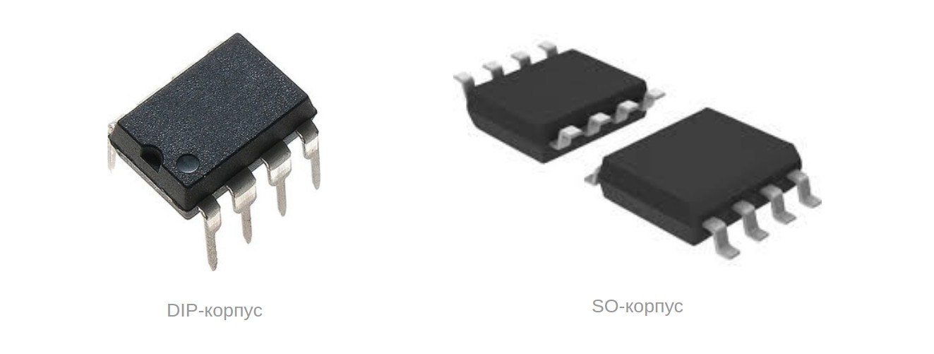
So, the scheme is done, the board is divorced. And then the first compromise is that Attiny85 microcontrollers are available in two types of enclosures - DIP (these are classic microcircuits with pin legs, which you probably saw at the dawn of electronic distribution and simple devices) and SO (these are planar microcircuits, small and compact, do not require additional holes for soldering and mounted on top of the board by soldering). At the time of designing, our supplier had a more expensive SO-version component and, most importantly, it was not available. Therefore, we took the DIP version, but with the expectation that we will first program it, and then carefully bite off the legs and solder it as SO, directly to the board. This made an additional technological risk - to change the firmware in this version after soldering the microcontroller to the board would not be a very trivial task, but who among us does not like difficulties ?!
We ordered the boards in China, this process is fine-tuned there, and we started collecting components. Light-emitting diodes and battery holders were also ordered in China, they either did not exist on the local market, or they were worth indecent money. The rest is bought in the nearest electronic supermarket. Microcontrollers could also be ordered in China, but a large number of negative responses and our own sad experience (when the components sent out did not provide enough good quality) kept us from taking this step. Therefore, by the time we received the finished printed circuit boards, the entire BoM was in our hands. There is even time left to slowly solder the programmer for microcontrollers.
After receiving the boards, we soldered one test device. Since the program for the microcontroller was postponed until the finished device was obtained (and it was right, I will tell you a little later), we did not solder the microcontroller “for good”, but made a transitional platform into which the chip can be plugged in like a light bulb into a cartridge. As expected, the device did not work. Looking closely at the device (for a couple of hours), we found an error - the LEDs were soldered incorrectly. The fact is that when mounting chips and elements with a large number of legs, it is very important not to confuse these legs and put the element correctly. To do this, the engineers on the markings on the printed circuit board use a key - an image of a point, which must coincide with the same one on the body of the chip. As a result, the process of soldering such an element looks like this - we combine the keys, solder one leg, solder all the others. To confuse the key is usually fraught with negative consequences - the author of these lines somehow shoved the microcontroller into the programmer from the wrong side - after five seconds the air smelled fried, and the finger that touched the chip got a neat burn according to the shape of the case. Fortunately, no one was hurt anymore and after cooling the microcontroller also remained working.
So, in the design of our board, we applied a self-made description for LEDs (three-millimeter SK6812s are rarely found than WS2812) and they safely made a mistake with the key. As a result, when mounting the LED key must be located on the other side relative to the key marked on the board. The test board went safely to the scrap.
The second test sample was already assembled with this error. Now we were sure that our scheme was operational and began to program the firmware.
It looked like this:
- microcontroller chip inserted into the programmer;
- firmware was poured into it;
- chip removed and inserted into the device;
- power on and performance checked;
- all repeated from the beginning.
I note that sometimes during the day this operation had to be repeated several dozen times. It was possible to solder the programmer directly to the chip on the board, but, as you remember, we are not looking for easy ways.
At the programming stage, too many interesting things came to light.
It all started with the fact that none of the standard libraries work with managed LEDs did not work. The reason was not in one place, but in two. Firstly, the time intervals for coding control signals were intended for other types of LEDs and did not coincide with the ones indicated in our documentation. Secondly, in the case of battery power, the microcontroller turns out to operate at a lower frequency and, by default, can reduce it even more to save energy (which it does when the battery is used), which again leads to a change in the time intervals for controlling the LEDs. A pair of clocks with an oscilloscope helped adjust the library to the required intervals, and half an hour and a few experiments allowed us to find a command that prohibits the microcontroller from changing the frequency of operation. As a result of a mid-term battle, we were able to manage the LEDs normally, lighting them with those colors that we needed, and not in a completely random order.
The second surprise was the light sensor. After programming it, we couldn’t understand for a long time why there was no reaction to closing it with a finger (i.e., completely darkening) from the word “absolutely”. The answer came after a few days of intently peering at examples of working with such sensors. It turned out that when setting up the analog port to which the sensor was to be connected, it was necessary to use one numbering, and when reading readings, another one (yes, I also remembered the anecdote “Wow, an error in one digit, and what a difference!”) . After this realization, everything worked as it should. The firmware has been written.
Since we were sent not one, and not two printed circuit boards, but ten at once (one, as we remember, was disposed of), we soldered all the others to the joy.
It turned out that the law of large numbers also works on small lots - two out of ten boards showed a manufacturing defect - our Chinese colleagues did not have a good electrical connection between the front and back layers of the board, as a result, nothing worked due to lack of power. Fortunately, this is easily eliminated by soldering the vias with the conductor.
The devices are assembled, tested and transferred for further processing to give the appearance of the finished decoration. In fact, we spent no more than a week on the whole development, but due to distractions to other tasks and expectations (free time, components, printed circuit boards) the whole process was spread over a half-year time interval.
If anyone is interested, the source code and project materials are laid out on Github .
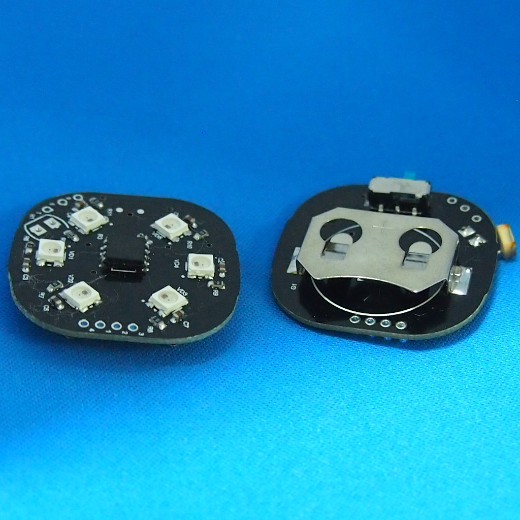
The story does not end there. After the first instructive experience, we made several versions of the board.
The second version was in two versions - with six LEDs in a circle and four (one in the center) and it was different in that here we used the SO-package of the chip. But even there it was not without excesses - when wiring the board because of the confusion in the names, the wrong contact area was chosen and as a result, the mounting feet of the chip had to be pressed under the case. In addition, they brought out the contacts for the firmware and the three "power-signal-ground" on separate platforms, in order to be able to add more LEDs as a remote element.
In addition, another unpleasant flaw was revealed - the master very much requested to make the board perfectly round (in our version it looked more like a rectangle with rounded corners). They did it, at the same time checking the Chinese industry on the production of boards thinner than a millimeter in thickness. The result was completely satisfactory - replacing the holders with those designed for CR2016 batteries, we got an even more lightweight platform from which you can already make, for example, earrings.
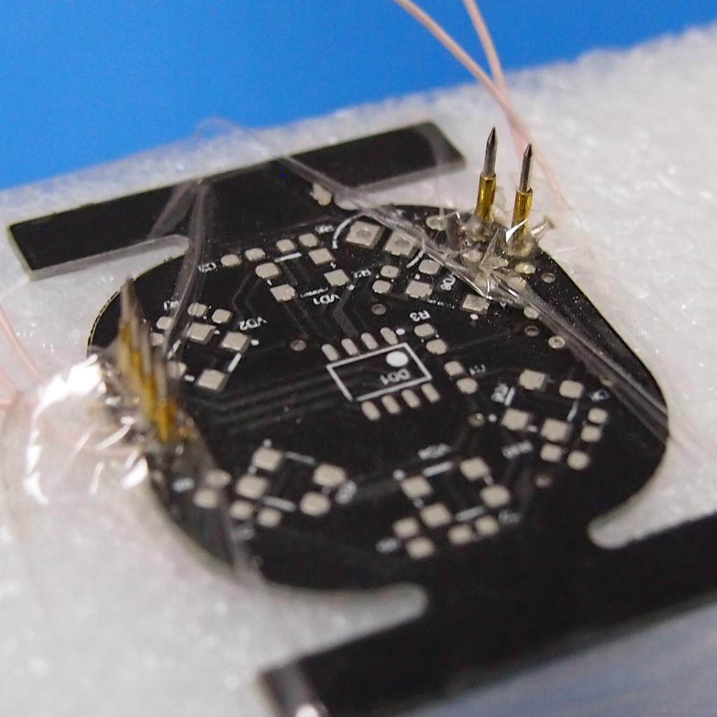
For the firmware of these devices, a programmer a la “collective farm” was used on pogo pins. As it turned out, the firmware download procedure was still non-trivial - you had to press the board tightly enough to the pins, which was not immediately possible the first time.
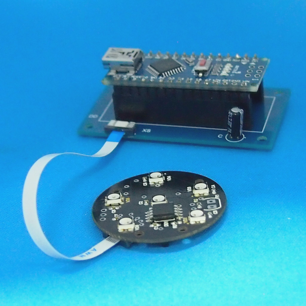
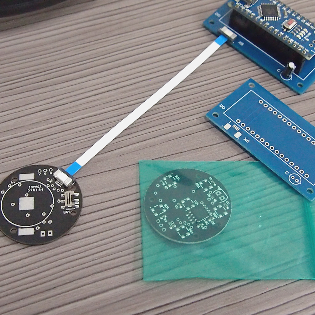
The apotheosis of the development of this branch of the platform was the third and latest version. In it, the contacts for the firmware were brought to a separate flexible cable, an additional fee was ordered for the programmer. At this iteration, we appreciated Seeedstudio's PCBA service, which made printed circuit boards for us — the Chinese industry brought the boards with most of the elements mounted, we soldered the connector for the programmer, the battery holder, the photoresistor and the LEDs - they were not (except for the photoresistor) components available for installation.
The result looks like this:
In general, the project turned out to be interesting. As it turned out, even seemingly simple things can conceal very complicated nuances inside, which was clearly shown.
All Articles