Revealing a 140-year-old secret in physics
Translation of an article by IBM Research.
An important breakthrough in physics will allow us to study the physical characteristics of semiconductors in much greater detail. Perhaps this will help accelerate the development of next-generation semiconductor technology.
Authors:
Oki Gunawan - Staff Member, IBM Research
Doug Bishop - Characterization Engineer, IBM Research
Semiconductors are the main building blocks of today's digital, electronic age, providing us with a variety of devices that benefit our modern life, such as computers, smartphones and other mobile devices. Improvements in the functionality and performance of semiconductors also enable the next generation of semiconductors to be used for computing, recognizing and transforming energy. Researchers have long struggled to overcome the limitations of our ability to fully understand electronic charges inside semiconductor devices and advanced semiconductor materials that hold back our ability to move forward.
In a new study in the journal Nature, a research co-authorship led by IBM Research describes a spectacular breakthrough in uncovering a 140-year-old mystery in physics, one that will allow us to study the physical characteristics of semiconductors in much greater detail and enable the development of new and improved semiconductor materials.
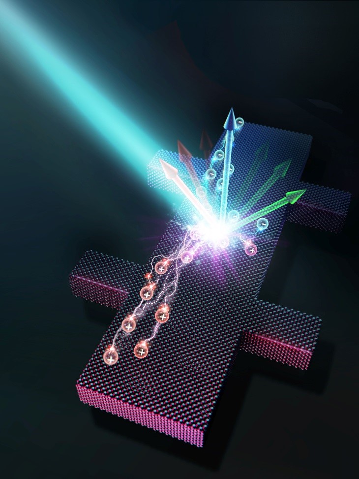
To really understand the physics of semiconductors, we must first understand the fundamental properties of charge carriers inside materials, whether they are negative or positive particles, their speed in an applied electric field and how densely they are packed in the material. Physicist Edwin Hall found a way to determine these properties in 1879 when he discovered that a magnetic field would deflect the movement of electronic charges inside a conductor, and that the deflection could be measured as the potential difference perpendicular to the directed flow of charged particles, as shown in Figure 1a. This voltage, known as the Hall voltage, reveals significant information about charge carriers in a semiconductor, including whether they are negative electrons or positive quasiparticles called “holes”, how fast they move in an electric field, or their “mobility” (µ) , and their concentration (n) inside the semiconductor.

140 year mystery
Decades after the discovery of the Hall, researchers also found that they could measure the Hall effect with light - experiments called the Photo Hall, see Figure 1b. In such experiments, light illumination generates multiple carriers or electron-hole pairs in semiconductors. Unfortunately, our understanding of the main Hall effect provided insight into only the main charge carriers (or majority carriers). Researchers were unable to extract the parameters of both carriers (primary and secondary) at the same time. Such information is key to many light-related applications, such as solar panels and other optoelectronic devices.
A study by IBM Research in the journal Nature reveals one of the long-held secrets of the Hall effect. Researchers from the Korea Advanced Institute of Science and Technology (KAIST), the Korea Research Institute of Chemical Technology (KRICT), Duke University, and IBM have discovered a new formula and technique that allows us to simultaneously extract information about the main and non-basic support, such as their concentration and mobility, as well as obtain additional information about the duration of the support, diffusion length and the recombination process.
More specifically, in a photo-Hall experiment, both carriers contribute to changes in conductivity (σ) and the Hall coefficient (H, proportional to the ratio of the Hall voltage to the magnetic field). Key insights come from measuring conductivity and Hall coefficient as a function of light intensity. Hidden in the form of a conductivity curve, the Hall coefficient (σ-H) shows fundamentally new information: the difference in the mobility of both carriers. As discussed in the article, this relationship can be elegantly expressed:
$$ display $$ Δµ = d (σ²H) / dσ $$ display $$
Starting with the known carrier density of most of the traditional Hall measurement in the dark, we can reveal for both majority and minority the mobility and density of carriers as a function of light intensity. The team called the new measurement method: Carrier-Resolved Photo Hall (CRPH), which was allowed by the carrier. With a known intensity of light illumination, the lifetime of the carrier can be set in a similar way. This connection and related decisions have been hidden for almost a century and a half since the discovery of the Hall effect.
In addition to the advances in this theoretical understanding, advances in experimental methods are also crucial to providing this new method. The method requires a clean measurement of the Hall signal, which can be difficult for materials where the Hall signal is weak (for example, due to low mobility) or when additional unwanted signals are present, as in strong light irradiation. For this, it is necessary to perform a Hall measurement using an oscillating magnetic field. As with listening to the radio, you must select the frequency of the desired station, discarding all other frequencies that act as noise. The CRPH method takes a step forward, and selects not only the desired frequency, but also the phase of the oscillating magnetic field according to a method called synchronous determination. This concept of an oscillating Hall measurement has long been known, but the traditional method using a system of electromagnetic coils to generate an oscillating magnetic field was ineffective.
Previous opening
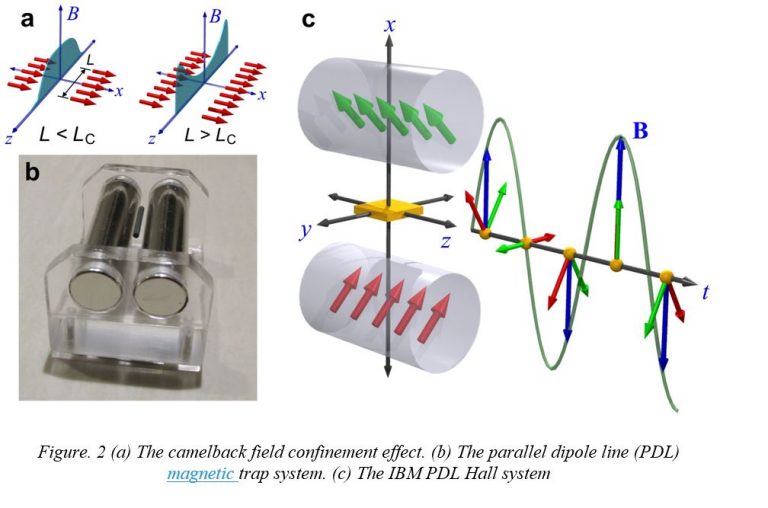
As often happens in science, advances in one area are caused by discoveries in another. In 2015, IBM Research reported a previously unknown phenomenon in physics related to a new magnetic field effect called the “camel hump” effect that occurs between two lines of transverse dipoles when they exceed a critical length, as shown in Figure 2a. The effect is a key feature that provides a new type of natural magnetic trap called the parallel dipole line trap (PDL trap), as shown in Figure 2b. PDL magnetic trap can be used as the latest platform for a variety of sensory applications, such as tiltmeter, seismometer (earthquake sensor). Similar new sensor systems, along with big data technologies, can open up many new applications, and are being studied by the IBM Research team, which is developing a big data analytics platform called the IBM Physical Analytics Integrated Repository Service (PAIRS), which contains a lot of geospatial data and the Internet of things Internet of Things (IoT).
Surprisingly, the same PDL element has another unique use. When rotated, it serves as an ideal system for a photo-Hall experiment to receive unidirectional and pure harmonic oscillations of the magnetic field (Figure Figure 2c). More importantly, the system provides enough space to allow illumination of a large area of the specimen, which is critical in photo-hall experiments.
Influence
The developed new method for the photo hall allows us to extract an amazing amount of information from semiconductors. Unlike only the three parameters obtained in the classical Hall measurement, this new method brings up to seven parameters for each of the tested light intensities. This includes the mobility of both electrons and holes; the concentration of their carrier under the influence of light; recombination lifetime; and diffusion length for electrons, holes, and ambipolar type. All this can be repeated N times (i.e., the number of light intensity parameters used in the experiment).
This new discovery and technology will help advance semiconductor advances in both existing and emerging technologies. We now have the knowledge and tools necessary to extract the physical characteristics of semiconductor materials with great detail. For example, it will help accelerate the development of next-generation semiconductor technology, such as the best solar panels, the best optoelectronic devices, and new materials and devices for artificial intelligence technologies.
The original article was published on October 7, 2019 on the IBM Research blog .
Translation: Nikolay Marin , Chief Technology Officer IBM in Russia and the CIS.
All Articles