The first experiments using the streaming protocol on the example of the connection of the CPU and the processor in the FPGA of the REDD complex
In previous articles, we already met with the Avalon-MM bus, where MM stands for Memory Mapped, i.e. projected onto memory. This tire is quite versatile. Several master (Master) and several slave devices can be connected to it. We already connected two leading devices at once (Instruction Master and Data Master), because the NIOS II processor has a Harvard architecture, so the command and data buses are different, but many authors connect them to the same common one to simplify software development from the outside to the bus.
If a block on the bus has direct memory access (DMA) functionality, it will also contain a master for the bus.
Actually, the main inconvenience of this tire is based on this fact (many leading, many followers). When we designed our slave, we had to decode the address. When I happened to make my leader, there was much more fuss with arbitration. But the assertion that development under Redd is an auxiliary part of the project, it should not require too many labor costs, is a red thread. And if we can free ourselves from the routine, we must free ourselves from it.

All articles in the series:
- Development of the simplest “firmware” for FPGAs installed in Redd, and debugging using the memory test as an example
- Development of the simplest “firmware” for FPGAs installed in Redd. Part 2. Program code
- Development of a proprietary core for embedding in a FPGA-based processor system
- Development of programs for the central processor Redd on the example of access to the FPGA
The Avalon Interface Specifications document already known to us (in general, I do not give direct links, since they always change, so the entire network is littered with articles with dead links, it’s easier to find the current position by driving the name into the search engine) reports that in addition to the Avalon-MM bus, there is also an Avalon-ST bus, where ST stands for Stream, that is, streaming. The fact is that very often the transmitted data has a stream structure. Yes, even the classic sector of the hard drive. It has a fixed size. It should be passed from beginning to end. Even if we consider it in the addressed area, the addresses will linearly increase. And if you use the FIFO block for storage, then the addresses inside it are completely hidden from us. They are, but working with them is not our concern.
The same applies to many other streaming data: they always go from beginning to end, being placed in repositories sequentially. This is exactly what streaming protocols are used for transferring such data. In addition to the lack of explicit addressing, the Avalon-ST bus is interesting in that it always connects two devices: a source and a receiver. There are always two of them. One device is always the source, the second is always the receiver. Therefore, problems with the arbitration of this bus do not concern. This is what typical pairs of devices connected to this bus look like:

And here are the typical signals of this bus:

Moreover, the error lines are optional, they transmit binary error codes assigned by us, and we can say that there are no error codes. And the channel number lines, as we saw above, are needed only if demultiplexing is performed further. If not, the channel number is not needed. We will do without it for now. Three lines remain: in fact, data, a ready signal and a data confirmation signal (strobe). Well, another clock signal, since the bus is synchronous.
From the documentation it also follows that three more signals are possible, adding to the bus the transmission properties of clearly defined packets:

In general, the tire is very interesting, and today we will begin experiments with it. As we already know, the FPGA is connected to the USB bus of the Redd complex via the FT2232H bridge operating in FT245-SYNC mode. Strictly speaking, the data passing through this interface is completely streaming data. Today we will learn how to transfer this data to our processor system based on NIOS II. It is a pity that the FT245-SYNC protocol, although streaming, does not fully comply with the Avalon-ST bus. To save chip legs, it has a bi-directional data bus, and the Avalon-ST bus is unidirectional. So, we have to make a block that coordinates close but not matching protocols.
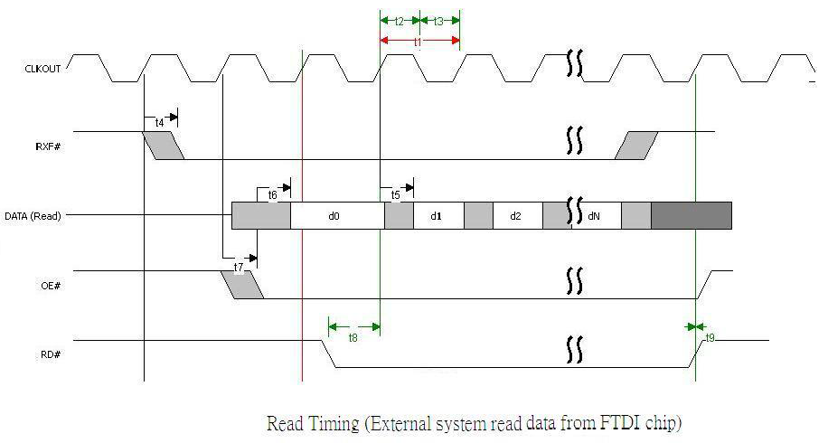
We already got acquainted with the FT245-SYNC protocol in one of the previous articles . Let me remind you that its description can be found in the document AN_130 FT2232H Used in an FT245 Style Synchronous FIFO Mode . Here is a typical timing diagram of the transmission from the bridge to the FPGA

In general, as a programmer, I am very interested in the fact that the transmitted package would have clearly marked start and end. Well, to make it more logical in logic to the UDP protocol, since if the transmission is in the TCP style, you will have to add special benchmark data to the stream, which will be spent on my programming, efforts and processor cycles ... It looks like the RXF line can help us with this. We check ... We fill in the “firmware” in the FPGA for measuring the performance, made in the previous article , and connect the oscilloscope probe to the RXF line. As a test program for the Redd central processor, we use the database, also used to measure performance, just instead of sending large amounts of data, we send a monolithic block of 0x400 bytes.
uint8_t temp [maxBlockSize]; memset (temp,0,sizeof (temp)); uint32_t dwWritten; FT_Write(ftHandle0, temp, 0x400, &dwWritten);
We get the following picture on the RXF line:

It is clear that the microcircuit receives 0x200 bytes of buffer (that is how much it can come in one USB2.0 HS packet), then it sends them to the channel. In general, this is strange, since the documentation states that two buffers are used in each direction. During the transmission, the second buffer should have had time to fill up. Alas. The end of its filling is clearly late. Actually, this shows why the performance does not reach the theoretical 52 megabytes per second: a large percentage of the time (although not 50%) simply does not transfer.
But one way or another, and we found out that it is possible to detect the beginning of a packet on a negative RXF edge only if the packet size does not exceed 0x200 bytes. If we send only commands with a small amount of data to the device, this is quite achievable. But if we send large streams of data, we will have to use a continuous channel, similar in its logic to UART (or, say, to the TCP channel), highlighting the packet boundaries purely programmatically.
In general, for simplicity of presentation, we take the streaming version as the basis. We will not consider packages today. Well, which version of the Avalon-ST bus we take as a basis is clear. We begin to design our block. As noted above, we have to make not just a bridge, but a switch, because the FT245FIFO bus is bidirectional, and the Avalon-ST bus is unidirectional. That is, it is necessary to make two Avalon-ST buses at once: output and input.

We are starting to slowly develop an automaton that will implement the logic we need. Of course, in the article this logic will be maximally simplified. Let's start with transferring data from the FPGA to the PC, since this process is a bit simpler (you do not need to switch the state of the OE line, which we talked about in the last article ). That is, we are implementing the Sink port.
From the side of the Avalon-ST bus, I chose the following mode of operation (there are a great many of them in the document, but this one is closest to the FT245-SYNC ):

Let me remind you the direction of the signals:

That is, we just wait for confirmation on the bus ( valid ), click on the data and gate this fact with the ready line.
From the FT245_FIFO side , the protocol looks like this:

It turns out that we must wait for the TXE signal and gate the data with the WR # signal (the polarity is inverse for both of these signals).
TXE # in its functionality is very similar to ready , and WR # is similar to valid . The details are a little different, but the logic is similar.
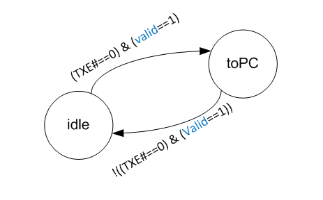
It turns out that we can single out one single state toPC, in which the simplest commutations of some lines will be performed. The condition for entering this state will be the readiness of both parties for transmission, that is (TXE # == 0) AND (valid == 1). As soon as some of the readiness is gone, we exit back to idle.
The transition graph of the automaton is still simple:
And the switching table is like this (where the signal names are ambiguous, indexes are added to them, where the names are unique - there are no indexes):
| Signal | ToPC status | Other conditions |
|---|---|---|
| WR # | NOT (validSink) | one |
| readySink | NOT (TXE #) | 0 |
| DATAFT245_FIFO | DataSink | Z |
Moving on to a slightly more complex transfer from Source to FT245_FIFO. As we saw in the previous article , the complication is switching the direction using the OE # signal:
For the Avalon_ST bus , everything is the same as before, so the pictures are not shown a second time, but now we are at the Source position.
Here, the RXF # line corresponds to the valid line, and the RD # line corresponds to the ready line. Well, fine, add a couple of states to the machine:
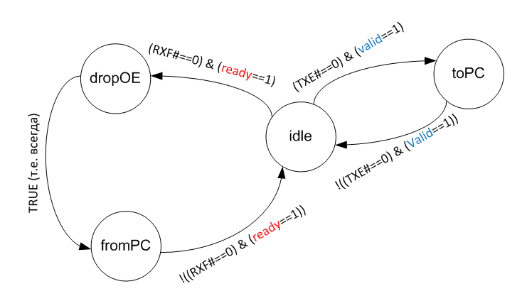
and the following logic for signals active in this state:
| Signal | dropOE | fromPC | Other conditions |
|---|---|---|---|
| OE # | 0 | 0 | one |
| RD # | one | NOT (readySource) | one |
| dataSource | Any value | DATAFT245_FIFO | Any value |
| valid source | 0 | NOT (RXF #) | 0 |
It is clear that the scheme was not the most ideal. There are various nuances associated with buffer overruns or underruns. But there shouldn’t be any kind of data loss, but as for optimality, you have to start somewhere!
We begin to transfer the developed theory to SystemVerilog code. True, we cannot use all the features of SystemVerilog. It was the case, I wrote a large article where I tested the practical synthesizability of the beautiful features of this language with a real development environment. Here we just ask for the use of interfaces, because the system will have two instances of the Avalon-ST type . Alas and ah. Here is the test code:
interface AvalonST #(parameter width=8)(input clk); logic [width-1:0] data; logic ready; logic valid; modport source (input clk, ready, output data,valid); modport sink (input clk, data, valid, output ready); endinterface module FT245toAvalonST ( AvalonST.source source, AvalonST.sink sink ); //assign source.ready = sink.valid; assign sink.ready = source.valid; endmodule
It is perfectly synthesized in the main compiler (a commented out line when deleting a comment causes an error to make sure that the synthesizer interprets everything correctly), but when checking the Analyze Synthesis Files button for a component for this code, an error is generated that the type AvalonST is unknown. That is, the analysis there is not on SystemVerilog, but on pure Verilog. It's a pity.

Moreover, the language is determined correctly, just the analyzer does not understand the interfaces among the ports.
In general, you have to use the ugly old syntax.
With this syntax we get the module interface:
module FT245toAvalonST ( input clk, input reset, inout [7:0] ft245_data, input logic ft245_rxf, input logic ft245_txe, output logic ft245_rd, output logic ft245_wr, output logic ft245_oe, output logic ft245_siwu, input logic source_ready, output logic source_valid, output logic[7:0] source_data, output logic sink_ready, input logic sink_valid, input logic[7:0] sink_data );
Rude, vintage, but what can you do.
We realize the transition graph of the automaton without any frills:
// enum {idle, toPC, dropOE, fromPC} state = idle; // always_ff @(posedge clk,posedge reset) begin if (reset == 1) begin state <= idle; end else begin case (state) idle: begin if ((ft245_txe == 0) && (sink_valid == 1)) state <= toPC; else if ((ft245_rxf == 0)&&(source_ready == 1)) state <= dropOE; end toPC: begin if (!((ft245_txe == 0) && (sink_valid == 1))) state <= idle; end dropOE: begin state <= fromPC; end fromPC: begin if (!((ft245_rxf == 0)&&(source_ready == 1))) state <= idle; end endcase end end
The control of the outputs, however, requires some explanation.
Part of the installations is done “on the forehead”:
// // , , // - . always_comb begin ft245_oe <= 1; ft245_rd <= 1; ft245_wr <= 1; source_valid <= 0; sink_ready <= 0; // , // assign- case (state) idle: begin end toPC: begin ft245_wr <= !(sink_valid); sink_ready <= !(ft245_txe); end dropOE: begin ft245_oe <= 0; end fromPC: begin ft245_oe <= 0; ft245_rd <= !(source_ready); source_valid <= !(ft245_rxf); end endcase end
But, say, for a bi-directional data bus, a typical solution should be applied. As we remember, it is declared in the interface part as follows:
inout [7:0] ft245_data,
and reading from it can be done in the usual way. For our case, we simply wrap all the data on the data of the outgoing Avalon-ST bus:
// assign source_data = ft245_data;
But in general, you can always read from the bus and in any way you like. But you should write to it using the multiplexer. When we write data to the bus, this data must come from any other bus prepared in advance. Typically, a variable of type reg (or newfangled logic ) is wound up in a module. In our case, such a bus already exists. This is the sink_data bus. In other cases, the state Z is output. If you are familiar with circuitry, you are well aware of the typical output buffer. It either skips any input data or goes into the Z-state. In our code, this multiplexer looks like this:
// inout- assign ft245_data = (state == toPC) ? sink_data : 8'hzz;
And another signal ft245_siwu. We never use it, so according to the documentation on FT2232H, pull it to unity:
// FTDI : // Tie this pin to VCCIO if not used. assign ft245_siwu = 1;
Actually, that's all.
The whole module looks like this:
module FT245toAvalonST ( input clk, input reset, inout [7:0] ft245_data, input logic ft245_rxf, input logic ft245_txe, output logic ft245_rd, output logic ft245_wr, output logic ft245_oe, output logic ft245_siwu, input logic source_ready, output logic source_valid, output logic[7:0] source_data, output logic sink_ready, input logic sink_valid, input logic[7:0] sink_data ); // enum {idle, toPC, dropOE, fromPC} state = idle; // always_ff @(posedge clk,posedge reset) begin if (reset == 1) begin state <= idle; end else begin case (state) idle: begin if ((ft245_txe == 0) && (sink_valid == 1)) state <= toPC; else if ((ft245_rxf == 0)&&(source_ready == 1)) state <= dropOE; end toPC: begin if (!((ft245_txe == 0) && (sink_valid == 1))) state <= idle; end dropOE: begin state <= fromPC; end fromPC: begin if (!((ft245_rxf == 0)&&(source_ready == 1))) state <= idle; end endcase end end // // , , // - . always_comb begin ft245_oe <= 1; ft245_rd <= 1; ft245_wr <= 1; source_valid <= 0; sink_ready <= 0; // , // assign- case (state) idle: begin end toPC: begin ft245_wr <= !(sink_valid); sink_ready <= !(ft245_txe); end dropOE: begin ft245_oe <= 0; end fromPC: begin ft245_oe <= 0; ft245_rd <= !(source_ready); source_valid <= !(ft245_rxf); end endcase end // - c , ... // FTDI : // Tie this pin to VCCIO if not used. assign ft245_siwu = 1; // inout- assign ft245_data = (state == toPC) ? sink_data : 8'hzz; // assign source_data = ft245_data; endmodule
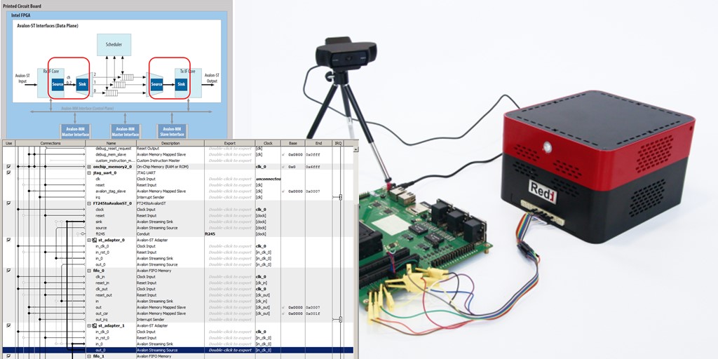
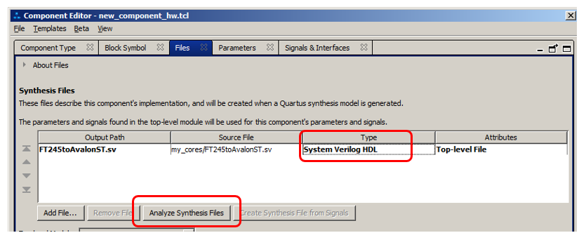
How to include the module in the list of available for use in the processor system, we examined in detail in one of the previous articles , so I just show the result in the figure. I recall that in order to achieve it, I had to add two AVALON-ST buses, one Conduit bus, pull signals from an erroneously defined AVALON-MM bus, and when there is not a single signal left in that bus, just delete it. Along the way, the figure shows the settings I selected for the AVALON-ST buses (8 bits per symbol, no errors, the maximum channel is zero, the latency is zero).

With the development of a module for docking tires - that's it. But alas, ah. To develop is only the beginning of work. Implementing is much harder. As you can see from the position of the scroller on the screen, the end of the article is still far away. So, we are starting to create a simple project that uses the FT245-SYNC bus joint with the AVALON-ST buses. It is the simplest. A serious project will not fit into the framework of a single article of a reasonable size. I will now simplify it by simplification just so that the readers' attention is enough for the rest of the text so that they do not quit reading in short. The first simplification is that 60 MHz clocks for the FT245_SYNC are generated by the FT2232H chip itself . I could add two clock lines to the system, but as soon as they see everything, we will have such cobwebs of wires that my mother does not grieve. If I still pay attention to different clock lines, we will all get confused. Therefore, I simply announce that today our processor system will clock from the FT2232H chip, and not from a regular generator.
Why can't you always do that? Very simple: as long as the FT2232H is not in 245_SYNC mode, it does not have these pulses at the output. That is, you must first run the program for the central processor, and only then load everything into the FPGA. If we were to create a system for an external customer, such a solution would create a lot of problems. I know from experience that they would regularly call us and say that nothing works, we would remind about bars, but that would help for a while. But we are doing an internal thing, and we will use it only in laboratory conditions. That is, within the framework of this task, this is permissible.
But it brings new challenges. We have a frequency of 60 MHz, and the SDRAM clock unit that we are currently using is tightly tied to a frequency of 50 MHz. Yes, I checked, 60 can be submitted, but let's pretend that we try not to go beyond the permissible modes. In subsequent articles I will try to show how to replace this hard block, but today we just say that since our clock unit from SDRAM cannot work on the used frequency, we exclude it from the SDRAM processor system. The program and its data will be fully located in the internal memory of the FPGA. It was experimentally found that in today's configuration, FPGAs can take up a maximum of 28 kilobytes of RAM for this business. It turns out that you can take volumes and not multiple powers of two ...
In addition, we will use the standard clock and reset unit. It is reset slightly different than the one we used for SDRAM. In order not to complicate the article, I will take advantage of the fact that the developed system will always work under the control of a debugger, so I will start a reset from the JTAG debugging subsystem.
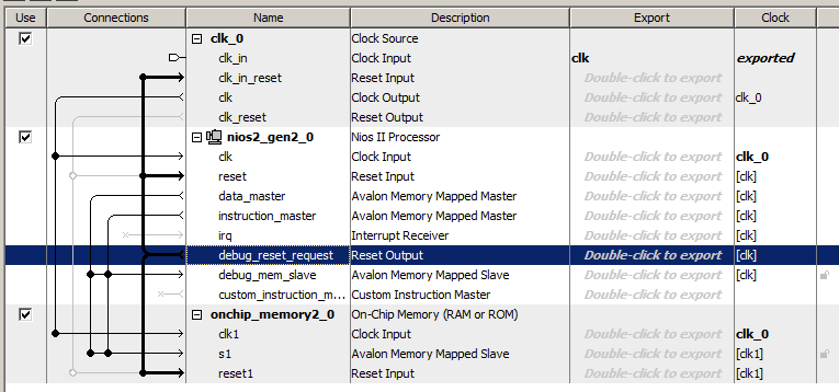
In total, we get such a sketch of the base processor system (the most difficult Reset line is highlighted at the moment, the blue marker is on the signal source):
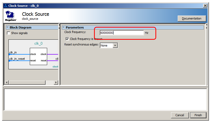
where the frequency has been adjusted for the clock and reset unit:
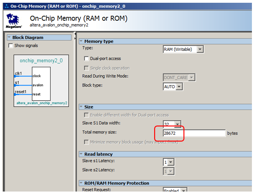
and for RAM - volume:
Today we need to display the text in the terminal. Therefore, we add the following interesting block to the system:
With this block, we will be able to call functions similar to printf. In addition to the AVALON_MM bus, it must also connect the interrupt request output.

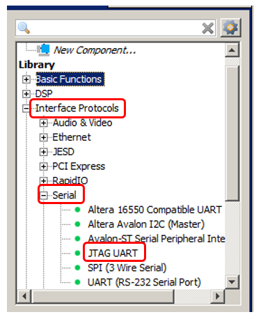
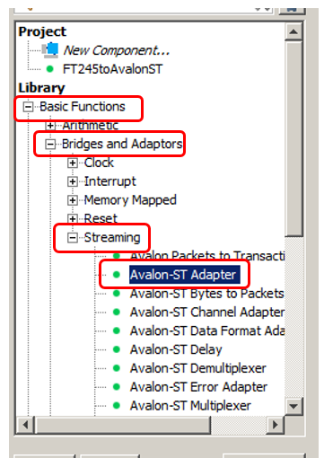
Everything, the procurement for the processor system is completed. It's time to embed our unit. Where will he send the data? Among the blocks available to us, there is a very interesting dual-port FIFO memory. Its charm is that one port can be configured to AVALON-ST mode and connect it to our unit, and the second to AVALON_MM mode and work with it using the NIOS II processor. This wonderful block is located here:

We have two Avalon-ST buses (one for reading, the other for writing), so we also need two FIFO blocks. Now I’ll go through one of them in great detail, we wind a couple of kilometers of web (and a bunch of text screens with pictures), and about the second we say that “it can be done by analogy”, indicating only differences. Therefore, so far we are adding only one block to the system and looking around at its settings. There are a lot of settings. One could simply indicate the required values so that everyone refers to the article as a reference, but suddenly someone gets into a situation that needs to be configured, but there is no access to the network (and, therefore, the article). Therefore, I will add settings iteratively. First obvious, then - as the system demands, run through the dialogue again and again. So everyone will feel the process and will be able to repeat it at any time. So. By default, we were given the following settings:
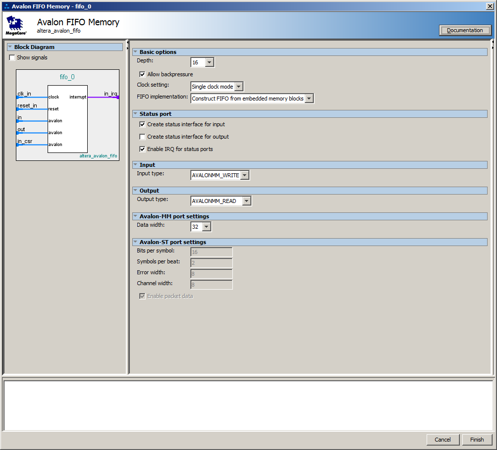
I will now do FIFO, which collects data from Avalon-ST , and uploads it to Avalon-MM . It turns out that the first edit will be like this:

I got this interesting warning:

It turns out that when at least one of the ports is projected onto the memory, the Avalon-ST bus width must be strictly 32 bits. And we have an 8-bit bus. How to agree on the bit depths, I'll tell you a little lower, but for now we are doing a 32-bit bus with an eight-bit character here. Well, disable batch mode, as was decided in the theoretical part.
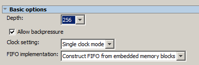
Next is the capacity. Suppose I make a queue for 256 words (i.e., 1024 bytes):
Now the status. At first, I did not attach any importance to it, and I got the program freezes tightly. So now I know that status is needed. Since we will work with the output port programmatically, we add a status for it.

and catch the error:

Well. Add double clocking. Just connect both inputs to the same clock line, since we have one.
Ufff. Total we have:

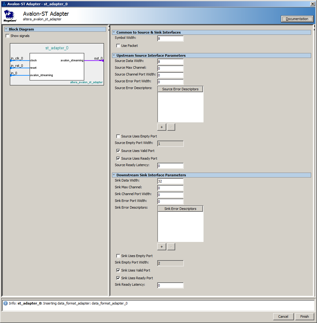
But it’s too early to connect this business to the common system. As we found out, the 8-bit Avalon-ST bus comes out of the block we developed, and this should include the 32-bit one. How do we be? Remodel your block? Not! Everything is already done before us. Here's what helps us:
Add it to the system. Moreover, since it is a layer, purely for beauty, we place it between our block and FIFO, using the corresponding arrow:

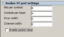
We do the following settings: on the input we have an 8-bit bus, on the 32-bit output. Packet signals are not used, ready and valid signals are used.
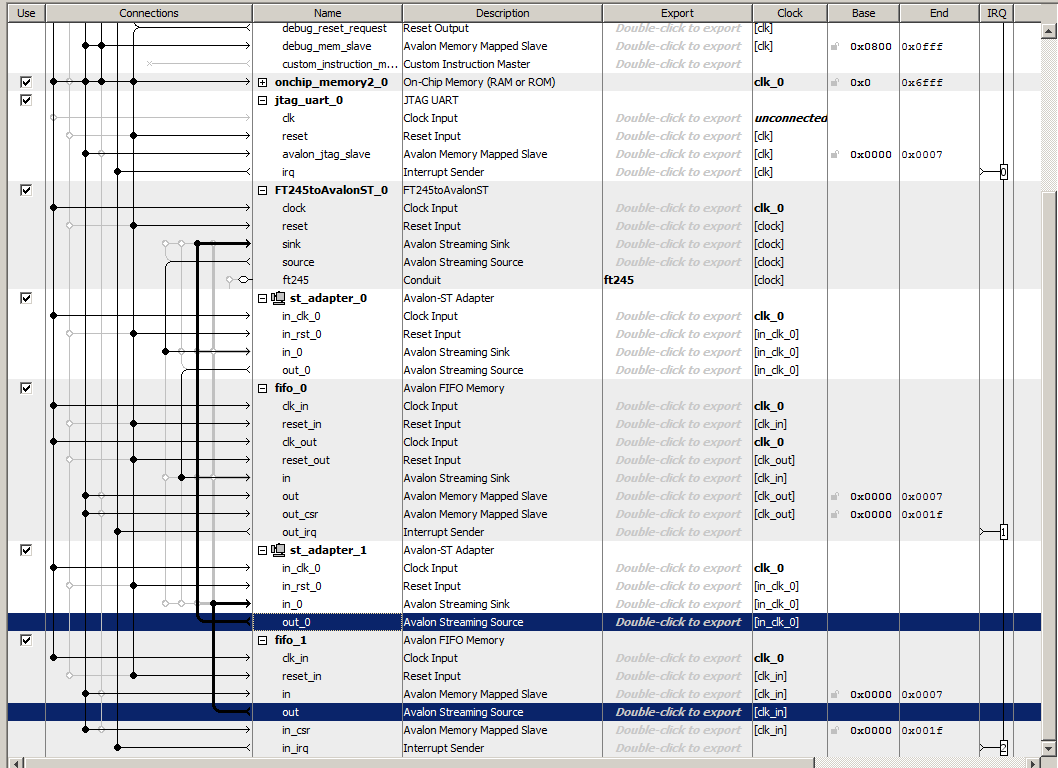
It's time to weave a web. First, I will lay the streaming lines (in the figure they are both highlighted, the markers are on the data receivers):

That is, the signal from the Source of our block goes to the input of the adapter. And from the adapter output to the FIFO input. As I said, all connections in the streaming protocol go on a point-to-point basis.
Well, now we hang the reset lines, clock lines, and also connect everything to the system bus and to interrupts ...

Well ... And now, by the same principle, we add FIFO to issue data to the FT245SYNC . Only there the data gets into the FIFO from Avalon-MM in 32-bit form. They pass through the 32-in-8 adapter and then get to the SINK input of our block, which is not connected in the current circuit ... We get the following fragment of the final circuit (the memory there turned out with a single clock):
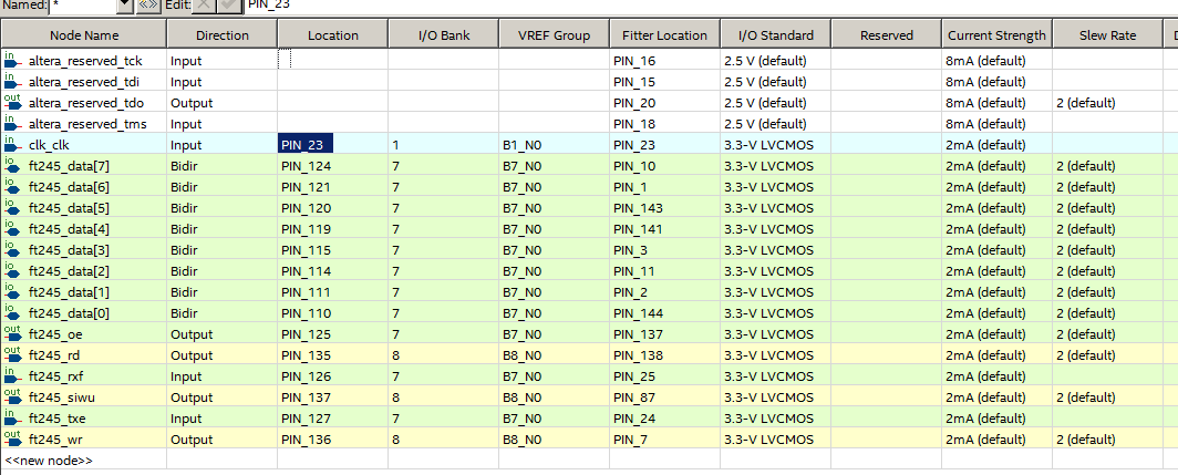
Further formalities that we have already worked out well in the experiments described in previous articles ( for the most part - in this one ). We assign vectors to the processor. For the system, we call the automatic assignment of interrupt numbers and addresses. We save the system ... Everyone remembers that the name of the saved system must match the name of the project so that the system is at the top level of the hierarchy? Add the system to the project, make a rough draft of the project, assign legs. Personally, I cheated: I copied the assignments from the * .qsf file of the draft project to the current finishing one (and you can take my project and copy the corresponding * .qsf lines to your own, but you can simply assign all the legs via the GUI). I pay special attention to the fact that the clk signal is connected to leg 23, not 25, as in previous projects. I remind you that here we are ticking from the FT2232 output.
Perfectly! The hardware is ready. We pass to the software. Where do we start? Today this question is not worth it. If we start with a program that runs on the NIOS II processor, nothing will work for us. First, we must put the FT2232 into 245-SYNC mode, only then our processor system will receive clock pulses. Therefore, we start with the code for the central processor.
We get something like this:
#include <cstdio> #include <sys/time.h> #include <unistd.h> #include "ftd2xx.h" FT_HANDLE OpenFT2232H() { FT_HANDLE ftHandle0; static FT_DEVICE ftDevice; // int nDevice = 0; while (true) { // if (FT_Open(nDevice, &ftHandle0) != FT_OK) { printf("No FT2232 found\n"); // , return 0; } // ? if (FT_GetDeviceInfo(ftHandle0, &ftDevice, NULL, NULL, NULL, NULL) == FT_OK) { // , if (ftDevice == FT_DEVICE_2232H) { // , AN130 FT_SetBitMode(ftHandle0, 0xff, 0x00); usleep(1000000); //Sync FIFO mode FT_SetBitMode(ftHandle0, 0xff, 0x40); FT_SetLatencyTimer(ftHandle0, 2); FT_SetUSBParameters(ftHandle0, 0x10000, 0x10000); return ftHandle0; } } // FT_Close(ftHandle0); // nDevice += 1; } printf("No FT2232 found\n"); } int main() { FT_HANDLE ftHandle0 = OpenFT2232H(); if (ftHandle0 == 0) { printf("Cannot open device\n"); return -1; } int item; bool bWork = true; while (bWork) { printf("1 - Send 16 bytes\n"); printf("2 - Send 256 bytes\n"); printf("3 - Receive loop\n"); printf("0 - Exit\n"); scanf("%d", &item); switch (item) { case 0: bWork = false; break; case 1: { static const unsigned char data[0x10] = { 0x00,0x01,0x02,0x03, 0x04,0x05,0x06,0x07,0x08,0x09,0x0a,0x0b,0x0c,0x0d,0x0e,0x0f }; DWORD dwWritten; FT_Write(ftHandle0, (void*)data, sizeof(data), &dwWritten); } break; case 2: { unsigned char data[0x100]; for (size_t i = 0; i < sizeof(data); i++) { data[i] = (unsigned char)i; } DWORD dwWritten; FT_Write(ftHandle0, (void*)data, sizeof(data), &dwWritten); } break; case 3: { DWORD dwRxBytes; DWORD dwRead; DWORD buf[0x100]; while (true) { FT_GetQueueStatus(ftHandle0, &dwRxBytes); if (dwRxBytes != 0) { printf("Received %d bytes (%d DWORDs)\n", dwRxBytes, dwRxBytes / sizeof(buf[0])); if (dwRxBytes > sizeof(buf)) { dwRxBytes = sizeof(buf); } FT_Read(ftHandle0, buf, dwRxBytes, &dwRead); for (DWORD i = 0; i < dwRxBytes / sizeof(buf[0]);i++) { printf("0x%X, ",buf[i]); } printf("\n"); } } } break; } } // , FT_Close(ftHandle0); return 0; }
The function OpenFT2232H () is familiar to us from the previous article . It is she who opens the FT2232 device and puts it in the mode we need. Immediately after the successful launch of the program, we get clock pulses, and with them the ability to debug the program for NIOS II. Well, the functionality of the main function is as simple as a stool. Send some data (1), send a lot of data (2), receive data (3). Please note that all data is sent in blocks that are multiples of four bytes. This is all because we have an 8-in-32 adapter. At the exit from it, the data should go in double words. Otherwise, everything is obvious.
When developing a program for NIOS II, you should first configure BSP. I remind you that I create the program itself according to the Hello World Small template. The changed fields in the BSP are marked in red in the figure below (how the program is created from the template and how the BSP is corrected was discussed in detail in one of the previous articles ). Let me remind you that I select the root of the tree, that is, the Settings element, so that all settings are immediately visible on the right.

Next, Generate BSP and, by virtue of my habit, I change the file name hello_world_small.c to hello_world_small.cpp , after which I clean up the project so that there are no induced errors from this renaming.
I’ll conduct a verification of the work quite superficially (a real tester would surely thoroughly test the transfer of large amounts of data exceeding the FIFO size, but the purpose of the article is to show the basic principles, and not to ensure that it is dropped to read due to its insane size). And I will show the basic principles in two stages. The first step is to verify data transfer from the central processor to NIOS II. For this, I developed the following code:
extern "C" { #include "sys/alt_stdio.h" #include <system.h> #include <altera_avalon_fifo_util.h> } #include <stdint.h> int main() { while (1) { int level = IORD_ALTERA_AVALON_FIFO_LEVEL(FIFO_0_OUT_CSR_BASE); if (level != 0) { alt_printf("0x%x words received:\n",level); for (int i=0;i<level;i++) { alt_printf("0x%x,",IORD_ALTERA_AVALON_FIFO_DATA (FIFO_0_OUT_BASE)); } alt_printf("\n"); } } /* Event loop never exits. */ while (1); return 0; }
This program is waiting for data to appear in FIFO. If they appeared there, displays them.
Getting to the test. First, I'll pretend I forgot to start the clock. Therefore, after turning on Redd, I load the FPGA “firmware”, then I try to run a debugging program for NIOS II. I get this message:
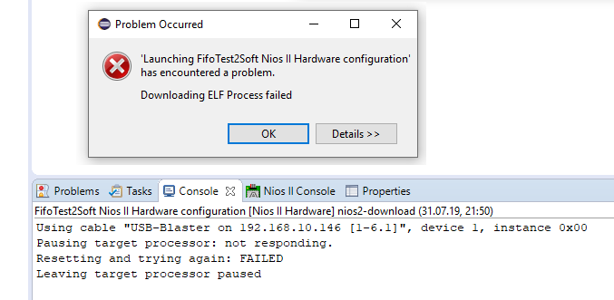
If you have the same, it means you really forgot to start clocking the processor system. But now you know how to quickly identify it. And to eliminate, it is necessary and sufficient to run the program that we wrote for the central processor. As soon as it starts and initializes the FT2232 bridge, clock pulses will go to our processor, and it will be possible to repeat the process of starting debugging. Moreover, the program for the central processor by that time can be completed. Clock pulses will not go anywhere: the bridge is already configured for FT245-SYNC mode .
In the program for the central processor, press 1. Depending on the situation, either appears in the terminal:
0x2 words received:
0x3020100,0x7060504,
0x2 words received:
0xb0a0908,0xf0e0d0c,
or:
0x3 words received:
0x3020100,0x7060504,0xb0a0908,
0x1 words received:
0xf0e0d0c,
In principle, there may be 1, then 3 double words, but this did not occur to me. It all depends on how many bytes have time to run on the bus before the first display begins. And if it started, then by the end of it all the other bytes will have time to run, since data transfer via JTAG is not a fast process. If the bus used packet signals, the program would be able to see the data only upon completion of packet reception. In some cases, it’s good (there is no packet yet, why should I see it? Especially if the packet is transitory), in some it’s bad (FIFO is a black box, for final processing the data should be copied to the addressable RAM, and this is better done in parallel with receiving data )
Transmitted data is placed in double words in Little Endian notation. Let me remind you that the following array is passed:
static const unsigned char data[0x10] = { 0x00,0x01,0x02,0x03, 0x04,0x05,0x06,0x07,0x08,0x09,0x0a,0x0b,0x0c,0x0d,0x0e,0x0f };
That's right. If you select item 2 in the program for the central processor, a message appears (for ease of reading, the lines are formatted when preparing the article):
0x3 words received: 0x3020100,0x7060504,0xb0a0908, 0x3d words received: 0xf0e0d0c, 0x13121110,0x17161514,0x1b1a1918,0x1f1e1d1c, 0x23222120,0x27262524,0x2b2a2928,0x2f2e2d2c, 0x33323130,0x37363534,0x3b3a3938,0x3f3e3d3c, 0x43424140,0x47464544,0x4b4a4948,0x4f4e4d4c, 0x53525150,0x57565554,0x5b5a5958,0x5f5e5d5c, 0x63626160,0x67666564,0x6b6a6968,0x6f6e6d6c, 0x73727170,0x77767574,0x7b7a7978,0x7f7e7d7c, 0x83828180,0x87868584,0x8b8a8988,0x8f8e8d8c, 0x93929190,0x97969594,0x9b9a9998,0x9f9e9d9c, 0xa3a2a1a0,0xa7a6a5a4,0xabaaa9a8,0xafaeadac, 0xb3b2b1b0,0xb7b6b5b4,0xbbbab9b8,0xbfbebdbc, 0xc3c2c1c0,0xc7c6c5c4,0xcbcac9c8,0xcfcecdcc, 0xd3d2d1d0,0xd7d6d5d4,0xdbdad9d8,0xdfdedddc, 0xe3e2e1e0,0xe7e6e5e4,0xebeae9e8,0xefeeedec, 0xf3f2f1f0,0xf7f6f5f4,0xfbfaf9f8,0xfffefdfc,
Everything is also true. We proceed to check the reverse gear. We replace the program for NIOS II with this:
/* - 2 */ uint32_t buf[] = {0x11223344,0x55667788,0x99aabbcc,0xddeeff00}; for (uint32_t i=0;i<sizeof(buf)/sizeof(buf[0]);i++) { IOWR_ALTERA_AVALON_FIFO_DATA (FIFO_1_IN_BASE,buf[i]); }
We select point 3 in the program for the central processor and run this version of the program for NIOS II. We get:
Received 16 bytes (4 DWORDs)
0x11223344, 0x55667788, 0x99AABBCC, 0xDDEEFF00,
Both channels work rough. And we’ll check it out some other time somehow.
Conclusion
This article discusses the basics of the Avalon-ST bus streaming protocol . Through this protocol, the connection of the Redd central processor with the processor system implemented in the FPGA is organized. Readers got an idea of the simplest method of interaction between the central and auxiliary processors. Download the projects created during the development process here .
However, the knowledge gained about streaming protocols and their use is very basic. In subsequent articles, it will be shown how through these protocols to efficiently save data in dynamic RAM located on the Redd board.
All Articles