About Intel Optane and Other Storage Options
I was interested in the aisergeev article about Intel with their 3D XPoint technology. The article states that this is an information storage technology that is not afraid of electron leakage, which is generally called non-volatile memory. It is great that such technologies come into our lives. Currently, among the solid-state non-volatile storage devices, usb flash and ssd are the most common. But, they have disadvantages in the form of this very electron leakage, which in turn imposes restrictions on the information retention period. It is obvious that Intel has released a fundamentally different type of memory, since the entry in it does not depend on electron leakage.
I was very interested in how exactly Intel created its memory. I searched the net and want to share with you the possible variants of this technology.
One of the first used digital types of memory without leakage is the now obsolete memory on magnetic domains - “Memory on magnetic cores” .
This technology is undergoing many ramifications and transformations. The most frequently mentioned ones are MRAM and STTRAM , MELRAM is also being developed , but this technology is being developed in a narrower, purely scientific circle (apparently it has not yet received commercialization).
MRAM (magnetoresistive random-access memory) magnetoresistive direct (random) access memory uses the quantum-mechanical effect of tunnel magnetoresistance , consists of a cell with two ferromagnets separated by a dielectric about 1 nm thick, a transistor reading the state (conductivity) of this cell and various types of state recording of this cell. The recording is made by electromagnetic induction.
This technology is very demanding on the size of the cell, since the electromagnetic field produced by the two conductors is quite large in size and at small cell sizes it will overlap the neighboring cells.
STTRAM - a random access magnetic memory with a torque ( STTRAM - random-access-memory spin-transfer-torque) is the same ( STT-MRAM - Spin-transfer magnetic random access memory).
The technology of this memory is based on spin electronics . The memory cells are semiconductor ferromagnets that change their conductivity from spin-polarized electrons applied to them. The top layer is a ferromagnet that changes its polarity from a spin-polarized current, the second layer is a barrier that changes its resistance to an electric current depending on the surrounding magnetic field, the bottom layer is a permanent magnet. If the direction of the magnetic fields coincides, the resistance of the barrier decreases, and vice versa increases if the directions of the fields differ. Perhaps this is a scientifically popular explanation for a semiconductor ferromagnet; perhaps the opposite is not enough information.
The reading of the state is made by measuring the resistance of the flowing current, the recording is made by applying a spin-polarized current. Functioning samples have a read / write speed of 20 ns and are made on 90 nm technology. The lowest read / write speed reached is 2 ns. Record current less than 200 nA. The resistance of the cell in the state "0" 2 kΩ, in the state "1" 4 kΩ. The technology allows multi-layer construction. The theoretical stability of reading / writing is more than 10 in 15 degrees, almost reached 10 in 13 degrees.
The current required for recording is more than an order of magnitude lower than that required in MRAM.
The first patents and the working cell were produced and registered by Grandis 2002-2009, the cell's operation, coupled with magnetic tunneling in 2004, is therefore not widely expected before 2024. But since the company, along with the patents, was acquired by Samsung, Samsung could be the first to launch this type of memory for sale.
This memory in the future is universal and will be able to replace the current memory and flash. Data on temperature stability is not, IMHO ~ -200 to +300 degrees.
Threat Spintronics is very promising in other areas.
The MELRAM cells of this magneto-electric memory are arranged as follows, the first part consists of a piezoelectric substrate, the second part is of a layered magnetoelastic material.
The first piezoelectric part has the ability to deform if a voltage is applied to them and a voltage is generated if they are deformed, the second part is magnetoelastic and strongly changes its magnetization during deformation. In working condition, when the electrical voltage is applied to the first part, the piezoelectric material is deformed and acts on the second part, the magnetoelastic material changes the magnetization to a perpendicular state, thereby recording occurs. Reading in this cell can be done in reverse order. Developed MIPT together with IRE them. V. A. Kotelnikov of the Russian Academy of Sciences and the International Associated Laboratory LIA LICS.
Resistive random access memory ( RRAM ), ReRAM. RRAM uses the effect of the ability of dielectrics under the influence of high electric voltage to become conductors, they are divided according to the type of impact on the dielectric and the size and location of the created conduction regions. According to the type of impact, there are bipolar switching when it is required to apply one polarity to the dielectric in order to switch it to high resistance and another to low resistance, and to unipolar switching, when different voltage levels are used to switch the state of the dielectric. Conduction regions can be either in the form of individual filaments, and not all of them will be conductors, or in the form of large zones that become conductors, also filaments and zones can be located either along the entire surface of the dielectric or only near the electrodes.
Memory cells can be connected directly or through selectors in the form of diodes or transistors. When assembling cells directly due to different conductivity of individual cells, it is very difficult to correctly assess the state of a particular cell, therefore a diode is connected to each cell, this minimizes electron leakage, but not completely, you can also switch on each cell through a transistor, it will increase speed and accuracy read the cell, but significantly complicate the structure, when connected only via diodes, you can create multidimensional 3d structures. This technology is rather young and is being developed by almost all major manufacturers of memory devices.
PCM - phase change memory (the same PCM, PCRAM, Ovonic Unified Memory, Chalcogenide RAM and C-RAM) memory based on the phase transition of a substance.
The working body of cells of this type of memory is chalcogenide , it would be better to call this substance more specifically - telluride. Tellurides of what exactly researchers use is not known; the wiki speaks of germanium and antimony; we can only assume that other rare earth metals are used, such as bismuth and beryllium. In different phase states, this substance conducts current in different ways, being amorphous, its resistance is high, in a crystalline state, the resistance is low and it easily conducts current. Currently, 4 stable states have been achieved from this substance, from crystalline to amorphous with two additional transition states, thanks to which the density of information storage increases substantially. Initially, in 1969, a switching speed of 100 ns was obtained from the material, and in 2006, 5 ns was achieved. In the same 2006, thanks to radiation resistance, the first commercial samples began to be used in space. Many satellites have stable orbits inside the Van Allen belts and for them radiation resistance is very critical.
But, PCM cells spontaneously switch from heating - they are afraid of high temperatures, and at low temperatures they should switch much slower or break down altogether. Which requires the creation of either a specific composition of telluride for certain temperatures, or temperature stable cell operation conditions.
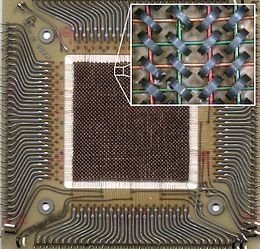
But back to Intel, and Intel uses PCM . But why this technology? Developed this technology and received the first patent by Stanford Ovshinsky , he generally developed a huge number of modern technologies used by us.
In 1970, in the September issue of Electronics, Gordon Moore - one of the founders of Intel - published an article about PCM. His personal interest and prompted the development of Intel in this direction. Since then, the terms of all primary patents in this area have passed, and now, almost 30 years later, other commercial organizations have taken part in further developments and improvements of this technology.
Optane - derived from the Latin captans (seizure, grip). Temperature modes of operation of the instruction manual Intel Optane:
Operating: 0 to 70 C
Non-Operating: -10 to 85 C
It is necessary to heat about 30 degrees above the maximum permissible and the information will not, it seems to be understandable, but why the lower storage threshold -10 degrees? Perhaps the cell will simply be destroyed as a glass jar of water in the cold.
PCM is permissible to use only in stationary equipment which is constantly warm and with proper cooling. In my opinion, this is an unacceptable method of storing information for laptops and other mobile equipment. Our winter freeze a laptop or phone below -10 degrees is easy and simple.
I was very interested in how exactly Intel created its memory. I searched the net and want to share with you the possible variants of this technology.
One of the first used digital types of memory without leakage is the now obsolete memory on magnetic domains - “Memory on magnetic cores” .
This technology is undergoing many ramifications and transformations. The most frequently mentioned ones are MRAM and STTRAM , MELRAM is also being developed , but this technology is being developed in a narrower, purely scientific circle (apparently it has not yet received commercialization).
MRAM (magnetoresistive random-access memory) magnetoresistive direct (random) access memory uses the quantum-mechanical effect of tunnel magnetoresistance , consists of a cell with two ferromagnets separated by a dielectric about 1 nm thick, a transistor reading the state (conductivity) of this cell and various types of state recording of this cell. The recording is made by electromagnetic induction.
This technology is very demanding on the size of the cell, since the electromagnetic field produced by the two conductors is quite large in size and at small cell sizes it will overlap the neighboring cells.
STTRAM - a random access magnetic memory with a torque ( STTRAM - random-access-memory spin-transfer-torque) is the same ( STT-MRAM - Spin-transfer magnetic random access memory).
The technology of this memory is based on spin electronics . The memory cells are semiconductor ferromagnets that change their conductivity from spin-polarized electrons applied to them. The top layer is a ferromagnet that changes its polarity from a spin-polarized current, the second layer is a barrier that changes its resistance to an electric current depending on the surrounding magnetic field, the bottom layer is a permanent magnet. If the direction of the magnetic fields coincides, the resistance of the barrier decreases, and vice versa increases if the directions of the fields differ. Perhaps this is a scientifically popular explanation for a semiconductor ferromagnet; perhaps the opposite is not enough information.
The reading of the state is made by measuring the resistance of the flowing current, the recording is made by applying a spin-polarized current. Functioning samples have a read / write speed of 20 ns and are made on 90 nm technology. The lowest read / write speed reached is 2 ns. Record current less than 200 nA. The resistance of the cell in the state "0" 2 kΩ, in the state "1" 4 kΩ. The technology allows multi-layer construction. The theoretical stability of reading / writing is more than 10 in 15 degrees, almost reached 10 in 13 degrees.
The current required for recording is more than an order of magnitude lower than that required in MRAM.
The first patents and the working cell were produced and registered by Grandis 2002-2009, the cell's operation, coupled with magnetic tunneling in 2004, is therefore not widely expected before 2024. But since the company, along with the patents, was acquired by Samsung, Samsung could be the first to launch this type of memory for sale.
This memory in the future is universal and will be able to replace the current memory and flash. Data on temperature stability is not, IMHO ~ -200 to +300 degrees.
Threat Spintronics is very promising in other areas.
The MELRAM cells of this magneto-electric memory are arranged as follows, the first part consists of a piezoelectric substrate, the second part is of a layered magnetoelastic material.
The first piezoelectric part has the ability to deform if a voltage is applied to them and a voltage is generated if they are deformed, the second part is magnetoelastic and strongly changes its magnetization during deformation. In working condition, when the electrical voltage is applied to the first part, the piezoelectric material is deformed and acts on the second part, the magnetoelastic material changes the magnetization to a perpendicular state, thereby recording occurs. Reading in this cell can be done in reverse order. Developed MIPT together with IRE them. V. A. Kotelnikov of the Russian Academy of Sciences and the International Associated Laboratory LIA LICS.
Next will be considered two completely different types of memory that do not use magnetic fields.
Resistive random access memory ( RRAM ), ReRAM. RRAM uses the effect of the ability of dielectrics under the influence of high electric voltage to become conductors, they are divided according to the type of impact on the dielectric and the size and location of the created conduction regions. According to the type of impact, there are bipolar switching when it is required to apply one polarity to the dielectric in order to switch it to high resistance and another to low resistance, and to unipolar switching, when different voltage levels are used to switch the state of the dielectric. Conduction regions can be either in the form of individual filaments, and not all of them will be conductors, or in the form of large zones that become conductors, also filaments and zones can be located either along the entire surface of the dielectric or only near the electrodes.
Memory cells can be connected directly or through selectors in the form of diodes or transistors. When assembling cells directly due to different conductivity of individual cells, it is very difficult to correctly assess the state of a particular cell, therefore a diode is connected to each cell, this minimizes electron leakage, but not completely, you can also switch on each cell through a transistor, it will increase speed and accuracy read the cell, but significantly complicate the structure, when connected only via diodes, you can create multidimensional 3d structures. This technology is rather young and is being developed by almost all major manufacturers of memory devices.
PCM - phase change memory (the same PCM, PCRAM, Ovonic Unified Memory, Chalcogenide RAM and C-RAM) memory based on the phase transition of a substance.
The working body of cells of this type of memory is chalcogenide , it would be better to call this substance more specifically - telluride. Tellurides of what exactly researchers use is not known; the wiki speaks of germanium and antimony; we can only assume that other rare earth metals are used, such as bismuth and beryllium. In different phase states, this substance conducts current in different ways, being amorphous, its resistance is high, in a crystalline state, the resistance is low and it easily conducts current. Currently, 4 stable states have been achieved from this substance, from crystalline to amorphous with two additional transition states, thanks to which the density of information storage increases substantially. Initially, in 1969, a switching speed of 100 ns was obtained from the material, and in 2006, 5 ns was achieved. In the same 2006, thanks to radiation resistance, the first commercial samples began to be used in space. Many satellites have stable orbits inside the Van Allen belts and for them radiation resistance is very critical.
But, PCM cells spontaneously switch from heating - they are afraid of high temperatures, and at low temperatures they should switch much slower or break down altogether. Which requires the creation of either a specific composition of telluride for certain temperatures, or temperature stable cell operation conditions.
But back to Intel, and Intel uses PCM . But why this technology? Developed this technology and received the first patent by Stanford Ovshinsky , he generally developed a huge number of modern technologies used by us.
In 1970, in the September issue of Electronics, Gordon Moore - one of the founders of Intel - published an article about PCM. His personal interest and prompted the development of Intel in this direction. Since then, the terms of all primary patents in this area have passed, and now, almost 30 years later, other commercial organizations have taken part in further developments and improvements of this technology.
Optane - derived from the Latin captans (seizure, grip). Temperature modes of operation of the instruction manual Intel Optane:
Operating: 0 to 70 C
Non-Operating: -10 to 85 C
It is necessary to heat about 30 degrees above the maximum permissible and the information will not, it seems to be understandable, but why the lower storage threshold -10 degrees? Perhaps the cell will simply be destroyed as a glass jar of water in the cold.
PCM is permissible to use only in stationary equipment which is constantly warm and with proper cooling. In my opinion, this is an unacceptable method of storing information for laptops and other mobile equipment. Our winter freeze a laptop or phone below -10 degrees is easy and simple.
Used materials
geektimes.ru/company/intel/blog/292093
https://ru.wikipedia.org/wiki/Memory_with changing_phase_state
https://ru.wikipedia.org/wiki/Memory_A_Magnitnyh_ coredechnik
https://ru.wikipedia.org/wiki/Spintronics
ru.wikipedia.org/wiki/%D0%A1%D0%BF%D0%B8%D0%BD%D1%82%D1%80%D0%BE%D0%BD%D0%B8%D0%BA%D0 % B0
en.wikipedia.org/wiki/Spin-transfer_torque
www.nkj.ru/news/31798
aip.scitation.org/doi/10.1063/1.4983717
mipt.ru/newsblog/lenta/uchyenye_sozdali_magnitnuyu_operativku
3dnews.ru/954365
3dnews.ru/954661
3dnews.ru/926712
3dnews.ru/557398
www.flashmemorysummit.com/English/Collaterals/Proceedings/2009/20090813_ThursPlenary_Tabrizi.pdf
dailytechinfo.org/electronics/6650-novye-fefet-tranzistory-smogut-obespechit-dalneyshee-soblyudenie-zakona-gordona-mura.html
All Articles