Progress on the foundry market - Samsung swings at TSMC
In the market for foundry services a small revolution is planned. Above the TSMC, which is still on the leader's pedestal, a shadow hung. We understand who, why and why “threatens”.
The entire market foundry is, no less than 50 billion dollars. This, of course, is not 350 billion. dale semiconductor manufacturing, but the piece is big enough.
Now half of the foundry market is covered by TSMC. But not so long ago, Samsung identified itself as a contender for a piece of foundry-business. The goal is clear: companies need to grow, and there are not so many growth directions.
The movement due to the growth of its own production, in particular, smartphones, cannot provide all the ambitions. It remains to master the adjacent directions.
Intel also makes gestures to the foundry sector, since the microprocessor market is not very growing, but I want to eat. But so far only Samsung shows real achievements.
To implement this strategy, the company singled out the foundry services in a separate direction, in order to avoid conflicts of interests of customers, and to better manage the business process. Still, business models are different, despite the common technological base. The division is not formal, Samsung Foundry has its own technological platforms.
(comment from the author: this is, by the way, one of the problems of manufacturing companies in Russia. Therefore, as well as foundation businesses, and it seems like IDM is in one bottle. Such a mix doesn't work normally. The customer will not place an order for a microcontroller for IoT at the factory, if the factory is a company engaged in IoT. Inevitably led to a conflict of interest).
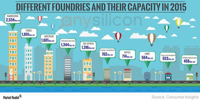
From the point of view of scale, Samsung is the best of all - the company has today the largest capacities in the number of plates, ahead of TSMC.
A separate area Samsung Foundry has three sites - two in Korea and one in the United States. Fab S1 (Giheung, Korea) launched in 2005, Fab S2 - (Austin) - introduced in 2011, Fab S3 (Hwaseong) - it is planned to start operating activities by the end of 2017. It is on this fab that production of techno-nodes 10, 8 is expected and 7nm.
The company backed up quantitative ambitions with an aggressive technological development roadmap (road map, which was shown to the public in May 2017).
The company intends to invest significant funds in order to achieve the technical process as much as 4nm faster than the main player foundry - the TSMC market.
Already in 2020, Samsung plans to begin the risk-production process 4nm. To replace the FinFET transistor structure, the company applies the first gate-all-around (GAA) FET design.
Samsung Foundry plans are quite ambitious:
- According to the results of 2017, go to the third place, pushing the UMC (now the company is in 4th place, if you count the DRAM orders).

- Cut off 25% of the total market foundry directions in the short term, “wringing” customers from TSMC.
True, there is still SMIC eager to fight, with a huge market and the support of the Chinese government. In any case, the market is waiting for redistribution in the next year or two.
The entire market foundry is, no less than 50 billion dollars. This, of course, is not 350 billion. dale semiconductor manufacturing, but the piece is big enough.
Now half of the foundry market is covered by TSMC. But not so long ago, Samsung identified itself as a contender for a piece of foundry-business. The goal is clear: companies need to grow, and there are not so many growth directions.
The movement due to the growth of its own production, in particular, smartphones, cannot provide all the ambitions. It remains to master the adjacent directions.
Intel also makes gestures to the foundry sector, since the microprocessor market is not very growing, but I want to eat. But so far only Samsung shows real achievements.
To implement this strategy, the company singled out the foundry services in a separate direction, in order to avoid conflicts of interests of customers, and to better manage the business process. Still, business models are different, despite the common technological base. The division is not formal, Samsung Foundry has its own technological platforms.
(comment from the author: this is, by the way, one of the problems of manufacturing companies in Russia. Therefore, as well as foundation businesses, and it seems like IDM is in one bottle. Such a mix doesn't work normally. The customer will not place an order for a microcontroller for IoT at the factory, if the factory is a company engaged in IoT. Inevitably led to a conflict of interest).
From the point of view of scale, Samsung is the best of all - the company has today the largest capacities in the number of plates, ahead of TSMC.
A separate area Samsung Foundry has three sites - two in Korea and one in the United States. Fab S1 (Giheung, Korea) launched in 2005, Fab S2 - (Austin) - introduced in 2011, Fab S3 (Hwaseong) - it is planned to start operating activities by the end of 2017. It is on this fab that production of techno-nodes 10, 8 is expected and 7nm.
The company backed up quantitative ambitions with an aggressive technological development roadmap (road map, which was shown to the public in May 2017).
The company intends to invest significant funds in order to achieve the technical process as much as 4nm faster than the main player foundry - the TSMC market.
Already in 2020, Samsung plans to begin the risk-production process 4nm. To replace the FinFET transistor structure, the company applies the first gate-all-around (GAA) FET design.
Samsung Foundry plans are quite ambitious:
- According to the results of 2017, go to the third place, pushing the UMC (now the company is in 4th place, if you count the DRAM orders).
- Cut off 25% of the total market foundry directions in the short term, “wringing” customers from TSMC.
True, there is still SMIC eager to fight, with a huge market and the support of the Chinese government. In any case, the market is waiting for redistribution in the next year or two.
All Articles