5 nm chip technology developed
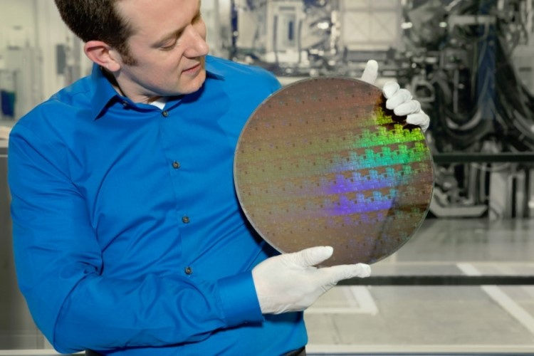
IBM has created a technology for the production of chips with a topology of 5 nanometers. The previous minimum, 7 nm, was announced two years ago. In production, the topology of 10 nm is now used, but this technology is not yet very common. For 10 nm technology, in particular, Snapdragon 835 chips are manufactured, which are installed in the Samsung Galaxy S8.
According to experts, 5 nm chips can significantly reduce the power consumption of devices, since such processors consume 75% less energy, but their performance is 40% higher than most current mobile chips manufactured using the 14 nm process technology. Thus, in offline mode, new devices will be able to work 2-3 times longer than now.
5nm technology is the fruit of IBM's joint work with Samsung and GlobalFoundries. The fact is that the corporation itself does not produce chips now, and GlobalFoundries and Samsung can license the technology. According to representatives of all partner companies, the technology will go into mass production by 2020, then at the same time new chips will begin to appear on the market. 14nm chips still prevail in electronics, the release of which began 2-3 years ago.
The developers decided to use a new type of transistors, which are combined into silicon nanosheets. Electrons are sent through four gates. The most advanced transistors of the FinFET type at the moment, which are massively used in the modern market, use three gates. Most likely, the FinFET technology will remain in the 7-nm chips, although over time it will go away, since it cannot be geometrically scaled. This was announced by IBM Research Vice President for IBM semiconductor technology Mukesh Khare.
“Going beyond 7 nm is very important. This is important both in constructive terms and in the fact that it is now possible to bring together more and more transistors. So we can talk about the 5 nm process, ”Hare said. The higher the density of transistors in the chip, the higher the speed of signals passing between them, respectively, the higher the speed of various tasks performed by such a chip.
For the production of new products, most likely, will be used photolithography technology in the deep ultraviolet (extreme ultraviolet lithography, EUV). The same technology was used to create test 7 nm chips. The width of nanosheets in the case of using this method can be adjusted. And fine tuning is very important in the production of chips. This cannot be achieved using FinFET.
A new achievement is extremely important both for society and for business. “For business and the community, cognitive and cloud computing are important, and they will improve with new advances in semiconductor technology,” said Arvind Krishna, head of IBM Research. He says that is why IBM is actively promoting new types of architectures and materials that push the boundaries of manufacturing capabilities.
All Articles