Took a video interview with Vice President Arduino and discussed with her teaching FPGA / FPGA school students and Verilog language
FPGA and boards can be used from any manufacturer (Xilinx, Altera, Lattice, Digilent, Terasic), everything I write below is not tied to this or that company.
Stanford teacher Svetlana Khutka took part in a conversation with Katy. She told Katy about the experiment on free training of schoolchildren in using FPGA in Kiev , by the efforts of enthusiastic teachers from several Kyiv universities. After that, I shared with Katy plans to conduct the next such experiment at the summer school of young programmers in Novosibirsk , well known from Soviet times, and also talked with other comrades from the Arduino community present about the implementation of FPGA in two schools and one Silicon Valley college.
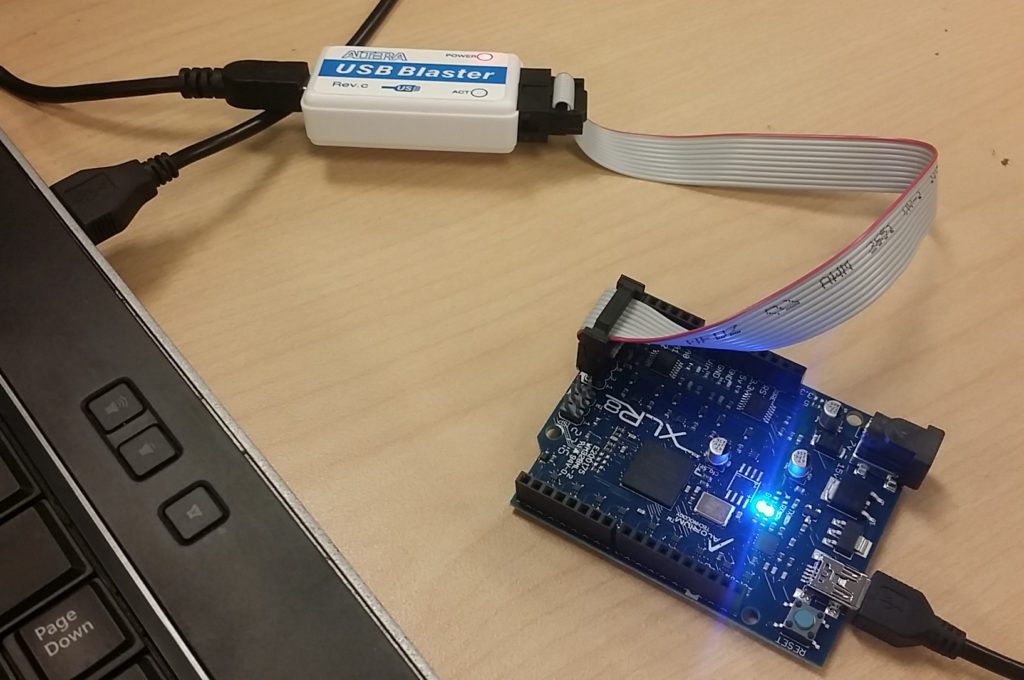
The FPGA board, which Katy now recommends, and which I am reworking to adapt it to my needs (there will be a separate post about it):
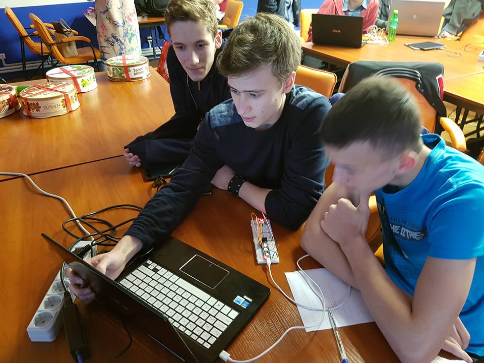
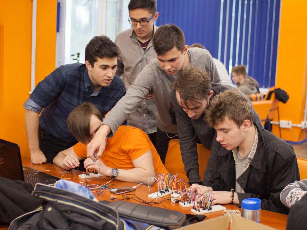
Below I will provide information on the results of the Kiev experiment, as well as some plans for the future, which are being developed by activists - teachers of physical schools and universities of Kiev, Chernihiv, Novosibirsk, Moscow, Nizhny Novgorod, Samara, St. Petersburg, Almaty and other cities. At the Kiev seminar, participants reached the creation of code-lock state machines and integration with simple peripheral devices (16-button keyboard, speaker). At the summer school in Novosibirsk, we will have more time and we will try to build a processor with the students. In the future, from this it is planned to make an annual course of the basics of digital electronics on FPGA for physical schools, which can enrich school education, as in the 1980s it was enriched by the introduction of programming elements.
Let's discuss this in detail:
1. Why teach schoolchildren language descriptions of equipment and the use of FPGA? Rationale for the program.
In the picture of the world represented by school education, there is a “blind spot” in the area of the principles of digital electronics design, between physics and programming. Robotics and arduino courses do not close this blind spot, since they boil down to programming ready-made chips. Exercises with discrete elements and microcircuits of a small degree of integration, although effective in the introduction to the basic principles, are based on the technologies of the 1960-1970s and do not contain a reference to modern design. The blind spot can be closed by introducing elements of the hardware description language (AEL) and FPGA chips (programmable logic integrated circuits) that are available for school experimentation — matrices of reconfigurable logic elements. Thus, the picture of the world becomes integral, and contributes to the creation of an environment for the emergence of a large number of young engineers who have an idea of all aspects of modern microcircuits for applications such as self-driving cars, and who are able to specialize in the future for designing one or another aspect of such devices.
The introduction of PLD and PLIS into the school curriculum is also well tied to the course of mathematics and physics of physical and mathematics schools - Boolean algebra, arithmetic circuits, finite automata.
Note that JADA and FPGA, despite the superficial similarities with programming, use other basic concepts:
Programming: sequential execution, select branches, cycles, variables, expressions, arrays (with the model of a flat addressable memory), functions (based on the use of the stack), recursion.
Designing digital logic: combinational logic element; construction of combining logic clouds from these elements, including selection primitives using multiplexers, as well as blocks for implementing arithmetic expressions; the concept of a clock signal for synchronizing calculations and repetition; the concept of a D-trigger for storing the current state between clock ticks; state machine; parallelism of operations, the hierarchy of modules, the concept of a pipeline (not only for the processor, but also for arithmetic units).
2. The general plan of such courses:
Section 1. Connection with physics, with laboratory on discrete components.
Section 2. Fundamentals of digital logic and arithmetic, with laboratory on chips with a small degree of integration.
Section 3. Designing circuits based on the synthesis of the instrument description language, with the laboratory on Xilinx or Altera FPGAs.
Section 4. Processor architecture: view from the programmer's side, with the laboratory using the RISC processor simulator at the instruction level, for example MARS MIPS.
Section 5. Microarchitecture: building a processor.
Individual project: integration of a sensor or other peripheral device with the circuit implemented in the FPGA.

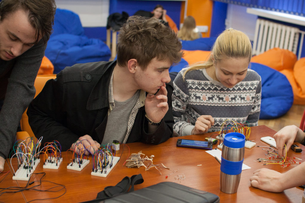
3. Results of the Kiev experiment.
Expanded text with the results of the Kiev experiment was written by a teacher of the Kiev Polytechnic Institute Yevgeny Korotky. I will supplement it with my personal conclusions. Prehistory - posts on Habré and Geektimes - 1 , 2 , 3 , 4 ). In those posts questions were asked. Here are the answers:
The hypothesis that schoolchildren can use Verilog has been confirmed
Verilog also turned out to be sufficiently interesting for schoolchildren (before Kiev, some colleagues doubted this, arguing that children were more interested in projects such as a robotic hand with a microcontroller)
The idea that, before using Verilog, it is useful to show schoolchildren logic elements and a D-trigger on chips with a small degree of integration - not exactly confirmed, but received more substantiation.
In total, after a day of experience with verilom, some schoolchildren started asking sensible questions - for example, when to use blocking, and when non-blocking assignment.
Bringing schoolchildren from zero to finite automata implementing protocols like SPI in one week is apparently unrealistic, but to the finite automaton of a code lock or traffic light is real.
It is also unrealistic to bring in one week on the design of the processor, but we will try to do it in two weeks in Novosibirsk.
During the Kiev experiment, we tried to talk about both FPGA and embedded processors (MediaTek MT7688, which is somewhere in the middle between Arduino and Intel Galileo or Rasberi Pay for performance). Then we made a hackathon (in the Kiev-Mohyla Academy) and observed how many students chose a project with FPGA for the hackathon and how many - a project with an embedded processor. It turned out - 50 to 50. This is interesting - until the hackathon, I had no idea what the breakdown would be.
I had a fear that schoolchildren might confuse the user interface in Xilinx Vivado, with a bunch of options and interface elements. But it turned out that the schoolchildren didn’t care - the complicated GUI didn’t scare them.
Most students use windows. Together with my colleague Alexander Belits, I have an idea to prepare for such events a couple dozen bootable SSD drives with Linux (Ubuntu or CentOS) and carry them from event to event. Alex even wrote a script for cloning such drives. Ubuntu is more friendly, but CentOS is more officially supported by FPGA design automation tools, in particular Xilinx Vivado and Altera Quartus. Is it possible to do both a Linux program and a Verilog / FPGA program during a summer camp? It is not clear, but you can try it.
It turns out that Xilinx Vivado mercilessly buggy configuration Artix-7 FPGA, if you use cheap badly shielded micro-USB cables. For some mystical inspiration, before my trip to Kiev, I shoved a dozen quality cords in my suitcase, and this was saved by a seminar.
I had the idea that using breadboardable FPGA modules (FPGA boards that plug into breadboard models), such as the Digilent Cmod A7 35T , can make it easier for students to switch from exercises with a small degree of integration to FPGA exercises. Whether this idea is true, I did not understand. It is possible to use larger boards with a rich set of peripherals, for example, Terasic DE10-Lite , will be just as good. Anyway, when switching from a low-integration chip (CMOS 4000 or 74HC) to FPGA, you need to change the supply voltage (from 9 V or 5 V to 3.3 V), so you cannot plug Cmod A7 instead of say CMOD 4013 into the same development board with lights and buttons, and expect that everything will continue to work.
I confirmed my observation that in order to conduct short-term (1 week) educational activities, it is critical that a brigade of students from a local university be in place to mentor schoolchildren. In the Kiev case, such a brigade was provided by Yevhen Korotky, a teacher at the Kiev Polytechnic Institute.
It became more or less clear in which cases and to what extent it is worthwhile to include in the program of such events a part about the level of transistors and about the production of microchips. This part was taught by Alexander Barabanov , an associate professor at Kiev National University, a translator of materials on the Nanometer ASIC course for students. Apparently, this material should be fully included in the annual course for schoolchildren, in a small one - in a two-week course in the summer camp format, but with a duration of less than a week you should probably immediately (for 1 hour after the start) give microchips of a small degree of integration (for example, CMOS 4000) and mentioning transistor casually, in the form “a transistor is a device in which a current flows from point A to point B if there is a voltage of 1 (or 0) in C. Logic elements AND, OR, NOT can be built from transistors (show on the picture) ”.
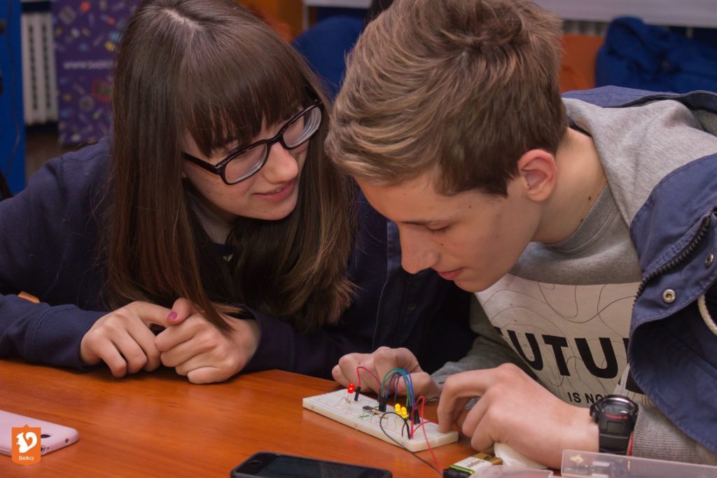
During lectures in front of a large audience, schoolchildren can be shown diagrams collected on a breadboard from microcircuits with a small degree of integration. This is clear, evoking interest, and also does not require connecting the structure to a computer - only with a 9 V battery. I showed three such schemes, the most critical for understanding is the XOR logic element, a 4-bit combinatorial D-trigger with a frequency of about 1 Hertz ( i.e. time per second).
It remains an open question whether it is possible to teach students the idea of pipelining, one of the most powerful ideas in digital design and organization of computation in general. To do this, it is not necessary to build a pipeline processor, you can make a pipelined arithmetic unit . Perhaps this can be mentioned at the very end of the course, when children play with simple combinational and sequential schemes and finite automata. Most likely it will be interesting to a very small subset of schoolchildren, but it's worth a try.
For events longer, you can use individual projects and verification work .
The code on GitHub used for the Kiev event

4. Sources of information for developing future materials.
Sources of information for teachers of physics and mathematics schools, which are likely to develop most of the detailed materials, after the initial experiments with schoolchildren in Ukraine, in Russia and in Silicon Valley:
Textbook by David Harris and Sarah Harris “Digital circuit design and computer architecture”, 2nd edition, Russian translation. This tutorial can be downloaded for free, see the articles on Habré about him - 1 , 2 , 3 . Recently, a new paper edition with improved color printing has also been released.
Slides for teachers, in addition to the textbook Harris & Harris. Free download.
Materials on the course From NAND to Tetris , which was created in Israel and implemented in some American universities. At the same time, IMHO, the course should use the ideas and the skeleton, but the implementation should be done on subsets of “adult” design tools, and not artificial “children's” tools, as the course does. Key parts are downloaded for free.
The book by Charles Petzold “Code”, which adequately explains many concepts on the fingers and the level of which corresponds to the school one (the idea is suggested by the teacher of the Kiev ORT school Sergey Dzyuba ). Again, from my point of view, ideas and a skeleton should be used from the book, but most of the material should be replaced by a more correct one (instead of latches (D-latch) use D-flip-flops (D-flip-flop)) and modern, for example instead of accumulator -based 6800 and archaic 8080 use a subset of the RISC architecture.
Kits for constructing circuits on a breadboard based on discrete components and low-integration chips from the American company ETron Circuit Labs, the Russian company Cyberphysics, the Ukrainian company Radiomag (I can explain the differences between these sets in the comments if anyone is interested).
Materials of manufacturing companies of FPGA chips (Xilinx, Altera) and educational boards with FPGA chips (Digilent, Terasic).
Code examples, test papers and project recommendations developed by Anton Moiseev, Yuri Panchul, Evgeny Korotky, Alexander Barabanov and other company engineers and university professors for various events in California, Kazakhstan, Russia and Ukraine.
5. Plan for the future number 1. The format of the annual course for 35 academic hours scattered for the academic year an hour a week
From physics to discrete elements
What is current, voltage and resistance. How is the breadboard. Exercise: the first circuit with a battery, LED and a resistor. Why include a resistor in the circuit with LED. Read labeling resistors. Variable resistors, photoresistors.
What is a transistor. Overview of switching elements from relays, radio tubes, discrete transistors to transistors on microchips. Exercises with thyristor (SCR - silicon controlled rectifier - more clearly than the transistor), bipolar pnp and npn transistors.
Test.
From discrete elements to combinational logic
Boolean algebra and logic algebra. Operations, expressions, axioms and identities, including the laws of de Morgan. Truth tables.
Combination logic elements AND, OR, NOT, AND-NOT, OR-NOT, EXCLUSIVE-OR (AND, OR, NOT, NAND, NOR, XOR). How combinational elements are built from transistors. Exercise: build AND, NAND or NOR from discrete elements.
Logic elements in chips of low degree of integration. Individual exercise: each student is given a personal logic chip from the CMOS 4000 series, with a technical description from the manufacturer, with the task to draw a truth table, demonstrate its work and verbally describe the function. Chips contain AND, OR, XOR, NOR, NAND logic elements with different numbers of inputs. What are pull-up resistors and why they are needed. Add to the previous exercise buttons and pull-up resistors.
Test.
Binary arithmetic and its implementation
Binary numbers. Convert from binary to decimal and vice versa. The operations of addition and multiplication. Negative numbers and additional code.
The implementation of a half-adder and a full adder using logic elements. Transfer Multi-bit transfer with successive transfer. Exercise on the breadboard. Mention of a long time delay and more optimal delay schemes.
Use of the 4-bit full adder CMOD 4008. Construction of an 8-bit adder and subtraction scheme from it. Homework for advanced students: study and make a presentation about the implementation of fast adders with accelerated group transfer.
Test.
Sequence logic
Building a clock signal generator based on the chip 555. Studying the effect of capacitors and resistances on the frequency and duration of the high and low levels.
Since capacitors in the 555 piping may require additional explanations of what capacitors are, why they are needed in the 555 piping and how they are labeled. An auxiliary exercise with charging and discharging capacitors of different capacities can also be useful.
Schemes with internal state. Building RS-latch of logical elements NAND. Study of the D-flip-flop behavior using the CMOS 4013 chip and the clock signal from 555 with a frequency of 1 Hz.
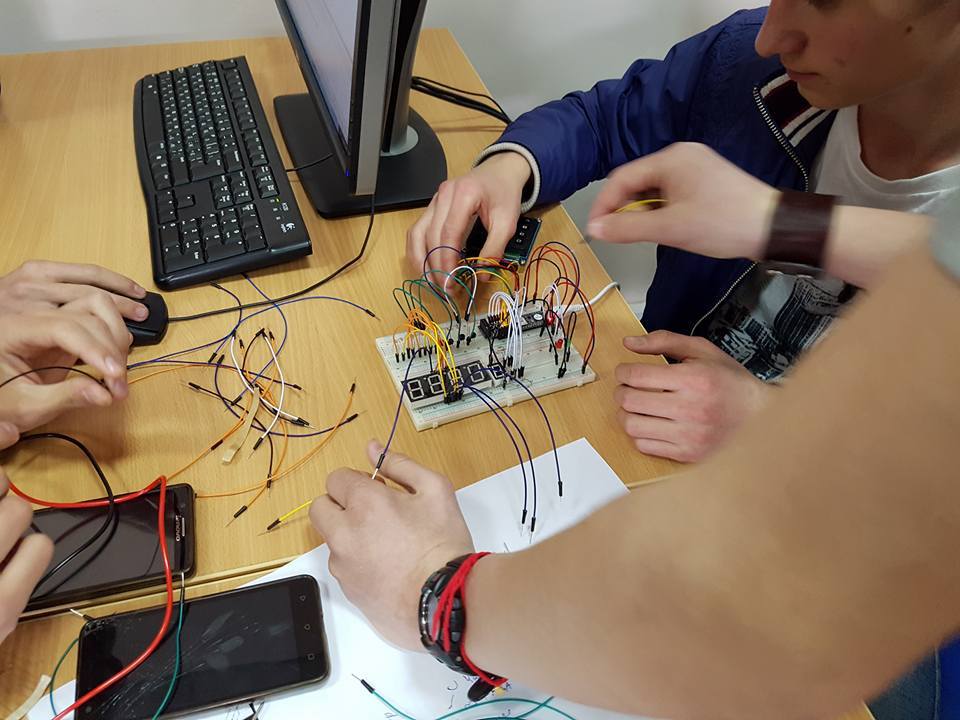
The sequential blocks are a counter (CMOS 4029) and shift register (4015). The seven-segment indicator and its driver 4511. Exercises with these microcircuits.
Exam.
From chips of low degree of integration to FPGA - combinational logic
The concept of FPGA (programmable logic integrated circuit) - a matrix of reconfigurable logic elements. Understanding Verilog hardware description language, synthesis, placement, tracing, and configuration procedures. Exercise: synthesis of the simplest combination module with the FPGA configuration on the training board.
Continue learning Verilog. Data types, expressions, assignments. Always-blocks and main operators. Exercise: display the first letters of your name and surname on the seven-segment indicator, switching between them using the button.
Continue learning Verilog. The hierarchy of modules. Exercise: building multiplexers and adders from submodules. Homework for advanced students: study and make a presentation about the implementation of fast adders with accelerated group transfer.
Simulation code on Verilog without FPGA. Subsets of the language for the implementation of the scheme and for its testing / verification. Simulation of time delays. Exercise: Creating an environment to test the operation of the schema described in Verilog. Using simulator Icarus Verilog for modeling and program GTKWave for viewing time diagrams.
Presentation of a group of advanced students: implementation of fast adders with accelerated group transfer, modeling time delays in them and comparing them with adders with sequential transfer (the number of logic elements and delays).
Test
Designing sequential logic in the language Verilog with implementation on the FPGA
Verilog language constructs that spawn D-triggers during synthesis. Explanation of the rules of design methodology at the level of register transfers: blocking and non-blocking assignments in various always-blocks. Simulation of sequential circuits on the simulator Icarus Verilog.
Exercises: implementation of D-flip-flop, counter and shift register on FPGA. Analysis of the results of the program of static analysis of the maximum frequency. Demonstration: Using sequential logic to generate audio signals and output them to a speaker.
The concept of a finite state machine. Diagrams of state changes. Exercises: endpoints for traffic lights and combination lock.
State machines for bus protocols. The choice of an independent project (with delivery at the end of the course) for the integration of sensors and other peripheral devices with the FPGA board. Independent work: an individual project that modifies the behavior of one of the examples with sequential logic: a counter, shift register or state machine.
Conveyor processing concept. Comparison of the pipeline implementation of arithmetic units that calculate the degree and the square root.
Test.
Processor architecture: view from the programmer’s side, with lab-based RISC processor-level simulator instructions, for example MARS MIPS .
The concept of background-Neymannovskoy machine. Introduction to assembler: commands, operands, registers, constants. Arithmetic and logical operations. Coding instructions. Exercise with a simulator processor at the instruction level - MARS MIPS. Simple assembler programs for evaluating expressions.
Conditional and unconditional jumps, labels, cycles. Example: calculating Fibonacci numbers. Individual exercise based on the modification of the example.
The concept of addressable memory. Instructions for loading and saving to memory. Assembly constructions for memory allocation. Exercise: a program that fills the memory with the calculated data. Individual exercise based on the modification of the example.
Test.
Microarchitecture: building a processor
An implementation on Verilog of a subset of the MIPS architecture with instruction memory, with general-purpose registers, but without data memory. The minimum instruction set is sufficient to calculate the Fibonacci numbers and the integer square root in an iterative way. Single-cycle microarchitecture. The simplest test environment with a hand-coded instruction array.
Continued 9.1
Submission of student sensor integration projects
Exam
6. Plan for the future number 2. Format of a two-week summer camp
Familiarity with the breadboard, resistances and logic elements.
The first circuit with a battery, LED and a resistor. Why include a resistor in the circuit with LED. Read labeling resistors.
Combination logic elements. Each student is given a personal logic chip series CMOS 4000, with a technical description from the manufacturer, with the task to draw a truth table, demonstrate its work and verbally describe the function. Chips contain AND, OR, XOR, NOR, NAND logic elements with different numbers of inputs. Inputs are connected to power and ground by adapters, and inputs and outputs are connected to LEDs.
Option exercise 2 with buttons and pull-up resistors, with an explanation of their function.
Introducing Binary Arithmetic
Using a 4-bit adder on a CMOD 4008 chip.
Build 8-bit adder from two 4-bit.
Construction of the subtraction scheme using the identity -a == ~ a + 1
Familiar with sequential logic
Building a clock signal generator based on the chip 555. Studying the effect of capacitors and resistances on the frequency and duration of the high and low levels.
Study of the D-flip-flop behavior using the CMOS 4013 chip and the clock signal from 555 with a frequency of 1 Hz.
Using the shift register to generate “running lights” based on CMOS 4015 chip.
We build a counter (CMOS 4029) and connect a seven-segment indicator to it via driver 4511.
Familiarity with the FPGA (programmable logic integrated circuit) - matrix of reconfigurable logic elements. Understanding Verilog hardware description language, synthesis, placement, tracing, and configuration procedures. Verilog data types, expressions, assignments. Always-blocks and main operators.
Synthesis of the simplest combination module with the FPGA configuration on the training board.
Output the first letters of your name and surname to a seven-segment indicator, switching between them using the button.
Continue learning Verilog. The hierarchy of modules. Simulation code on Verilog without FPGA. Subsets of the language for the implementation of the scheme and for its testing / verification. Simulation of time delays.
Exercise: building multiplexers from submodules.
Creating an environment to test the operation of the scheme described in the Verilog language. Using simulator Icarus Verilog for modeling, as well as the program GTKWave for viewing time diagrams.
Designing sequential logic in Verilog. Verilog language constructs that spawn D-triggers during synthesis. Explanation of the rules of design methodology at the level of register transfers: blocking and non-blocking assignments in various always-blocks. Simulation of sequential circuits on the simulator Icarus Verilog. Analysis of the results of the program of static analysis of the maximum frequency.
The implementation of the counter on the FPGA.
Implementation of the shift register on the FPGA.
Using sequential logic to generate audio signals and output them to the speaker.
Modification of exercise 2 or exercise 3 on the basis of an individual task.
The concept of a finite state machine. Diagrams of state changes. . ( ) c .
“ ”.
.
.
: . - . MARS MIPS .
: , , , . . . .
, , . .
. . . , . .
: .
Verilog MIPS , , . , , . . .
.

Appendix A. What is the hardware description language Verilogi and how it is associated with the design of microcircuits
From the post on Geektimes The squires of microelectronics. Video report from an electronics design conference in San Francisco.
25 Verilog ( — VHDL), (logic synthesis) , (static timing analysis) , , (place-and-route) .
: , , , , static timing analysis, floorplanning, place-n-route, parasitics extraction .. — GDSII, , . Taiwan Semiconductor Manufacturing Company TSMC.
Appendix B. What is FPGA / FPGA and why the study of FPGA cannot be replaced by a deeper study of Arduino or Rasberry Pie?
From the post on Habré How to start developing iron using FPGA - step by step instruction :
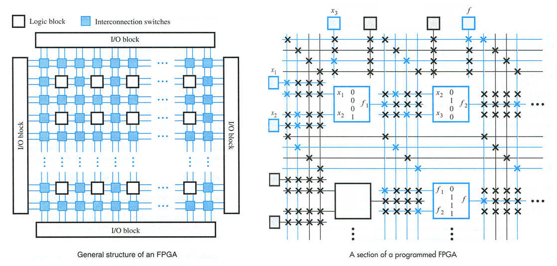
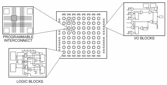
FPGA , , . AND , — .. — FPGA , , ..
- / FPGA — , «» ( -) (), ( ) ().
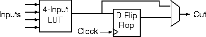
— FPGA, look-up table (LUT) flip-flop. , , .
, FPGA:
:
C. ,
(system on chip, SoC), IP- (CPU, GPU, DSP) — , . ADAS (advanced driver-assistance systems) .
, , , ( 1980- — 1990- ). (hardware description languages — HDL), (register transfer level — RTL), RTL-to-GDSII, Verilog VHDL , FPGA (field-programmable gate arrays). , -, -. HDL RTL , , , , 1980- .
In addition to the conference in Tomsk and the planned next experiment in July in Novosibirsk, which is supported by the Novosibirsk Summer School for Young Programmers, there is still an early plan to organize such an experiment in Kazakhstan (this is particularly interested in Venera Zhanalina who attended the Kiev seminar).
Appendix D. Examples of the simplest code on Verilog and the schemes it generates
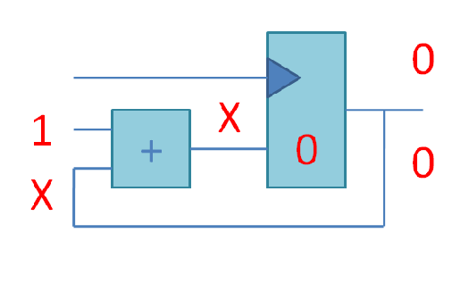
module adder ( input a, input b, input carry_in, output reg sum, output reg carry_out ); reg p, q; always @* begin p = a ^ b; q = a & b; sum = p ^ carry_in; carry_out = q | (p & carry_in); end endmodule

module counter ( input clock, input resetn, input load, input [15:0] load_data, output reg [15:0] count ); always @ (posedge clock or negedge resetn) begin if (! resetn) count <= 0; else if (load) count <= load_data; else count <= count + 1; end endmodule

How it works: A
detailed explanation is in the text “Introduction to the design of hardware chips for those programmers who have never done this” .
If you are a teacher and want to participate in the development of such materials (this is all on a volunteer basis, without contacting one company or another), let me know in the comments. Any criticism is also interesting.

All Articles