
最後に、私の手はFPGAの研究に到達しました。 そして、どういうわけか間違っていることがわかりました。Linux用のハードウェア用のドライバーを作成し、マイクロコントローラーをプログラムし、回路を読んで(そして少し設計します)、さらに成長する必要があります。
LEDを点滅させるのは面白くないように思えたので、簡単なことをすることにしました。 つまり、UART用のレシーバーとトランスミッターモジュールを記述し、FPGA内でそれらを組み合わせて(同時にIPコアの使用方法を理解します)、すべてを実際のハードウェアでテストします。
私は、タスクの普遍的なパラメーター化されたコアを作成することはタスクではなかったことをすぐに言います。 これは単なるテストプロジェクトであり、「FPGAとは何か、それと通信する方法を感じてください」というテーマに基づいています。
それでは、受信機から始めましょう。 アルゴリズムはかなりよく説明されているので、ここではその主要な点のみを繰り返します。
- RX信号のサンプリング周波数は、必要なUART伝送速度の4倍です。
- 受信が開始されない条件は、受信が現在進行中でない場合、入力信号RXが高レベルから低レベルに遷移することと見なされます。
- スタートビットを確実に識別するための条件は、サンプリング周波数の2番目のクロックサイクルでRX信号がLow状態に保持されることです。 同時に、実際にはビットパルスの中間に位置するため、4サイクルごとにパルスをさらにサンプリングできます。
- スタートビットまたはストップビットにエラーがある場合、エラー信号エラーを設定します。 それに基づいて、fastsync信号を形成します。これは、将来の高速受信機同期に使用します。
- 開始ビットを識別した後、最も若いものから順にデータビットの順次受信を開始します。 受信したデータは、1ビット右にシフトしてレジスタに書き込まれます。 受信終了の条件は、シフトレジスタの0番目の位置でのスタートビットの検出です。
- 受信機の迅速な同期は、RX信号が高レベルになったときにエラーを検出した後、元の状態にすることで構成されます(これは、論理「1」送信、ストップビット送信、または送信ラインの非アクティブ状態のいずれかです)。
- 受信が正常に完了する条件(スタートビットとストップビットの正しい値)は、完全な信号です。 それから(rdclk信号でクロックされた場合)、rxdataバス上の有効なデータの存在を示すレディパルス信号が生成されます。
次のデータ処理の速度をUARTの交換レートに結び付けないように、clkクロック信号から読み取り信号の準備を整えたくありませんでした。 同様の実装が送信モジュールにあります( 以下を参照 )。 レシーバーとトランスミッターモジュール間のテスト接続は、IntelのIPコアFIFOに基づいており、消費者とデータジェネレーターの異なる速度をシミュレートする機能を備えています。 唯一の制限は、データのプロデューサーとコンシューマーのクロック周波数がクロック周波数clkより低くてはならないことです。
受信モジュール(Verilog)
// // UART // // rxdata , ready==1 error==0. // ready 1 rdclk. // // : // rx // 2- . , . // 8 - ( 9 ). // 2 - , // . // // . // . '0' , . '1' // idle (. '1') // start- (. '0') // stop- (. '1') module uart_rx( nreset, // (, 0) clk, // UART, .. UART rx, // UART rdclk, // (rxdata, ready) rxdata, // , ready==1 ready, // rxdata ( 1) error, // ( 1) busy, // ( , 1) idle); // ( 1) input wire nreset; // (, 0) input wire clk; // , .. UART input wire rx; // UART input wire rdclk; // output wire[7:0] rxdata; output wire ready; output error; output busy; output idle; // , rdclk reg[2:0] done = 3'b000; // , rdclk //assign ready = (done == 2'b10) ? 1'b1 : 1'b0; assign ready = (done[1] && !done[0]) ? 1'b1 : 1'b0; // reg error = 1'b0; // // error // rx, . wire fastsync = (error && rx); // reg idle = 1'b1; // : // d[9] - , .. == 1 // d[8:1] - // d[0] - , .. == 0 reg[9:0] d = 10'b1xxxxxxxx1; // . 2'b10 wire[1:0] status = { d[9], d[0] }; // . wire complete = (status == 2'b10) ? 1'b1 : 1'b0; // assign rxdata = d[8:1]; // reg busy = 0; // rx reg[1:0] cnt; always @(posedge clk, negedge nreset) begin if(!nreset) begin rxreset(); end else begin if(fastsync) begin rxreset(); end else begin if(busy == 1'b1) begin // -, rx if(cnt == 2'd0) begin // // // (.. ) d <= { rx, d[9:1] }; if(d[1] == 1'b0) begin // , busy <= 1'b0; // error <= (rx == 1'b1) ? 1'b0 : 1'b1; end else begin // if(rx && (d == 10'b1111111111)) begin // busy <= 1'b0; // error <= 1'b1; end else begin // // - - cnt <= 2'd3; end end end else begin // - cnt <= cnt - 2'd1; end end else begin // if(!error) begin // , if(rx == 1'b0) begin // - busy <= 1'b1; // . 1, .. // d[0]==0 d <= 10'b1111111111; // rx 1/2 // 1- - // 2- - (cnt 0) cnt <= 2'd0; // .. , idle <= 1'b0; end else begin // idle <= 1'b1; end end end end end end task rxreset; begin // error <= 1'b0; // (!?) idle <= 1'b1; // busy <= 0; // -, complete d <= 10'b1xxxxxxxx1; end endtask always @(negedge rdclk, negedge nreset) begin if(!nreset) begin done <= 3'b000; end else begin // complete. // ready // complete 0 1 rdclk. done <= { complete, done[2:1] }; end end endmodule
入力信号RXは非同期で(おそらく)不安定なので、 多数の要素がメインモジュールの受信モジュールの前に接続されました。 要素もVerilogで記述されていますが、そのコードはここでは意味がありません。 代わりに、合成された要素の美しい写真。
多数要素の合成スキーム 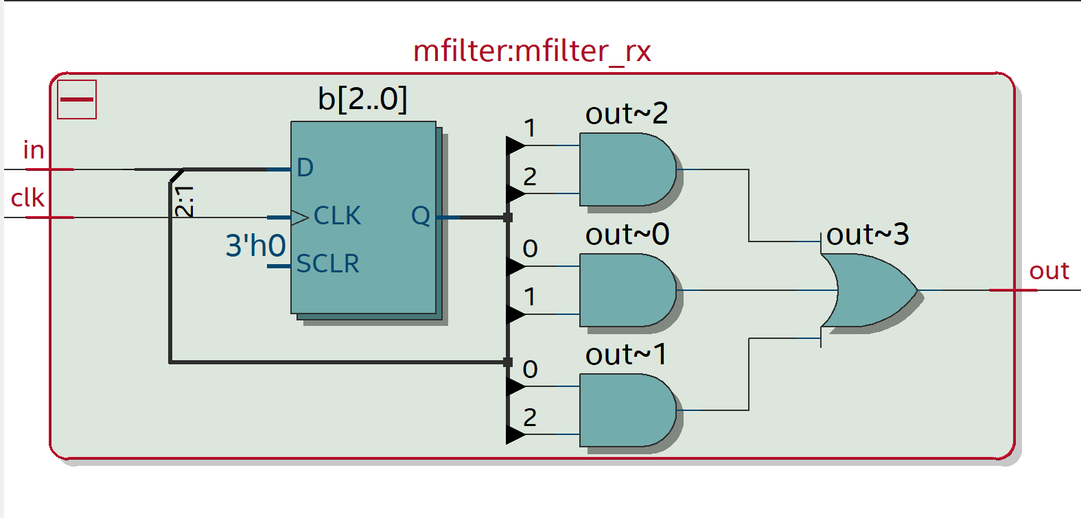
送信機ユニットはさらにシンプルであり、追加のコメントは不要だと思います。
トランスミッターモジュール(常に内部でのVerilogのブロックおよび非ブロックの割り当て)
// // UART // // : // clk - 4 , // rdclk - txdata, write, fetch. .. clk // txdata - , write/fetch // write - (1=) // fetch - (1=) // tx - UART // idle - (1=, ) // // FIFO dcfifo_component.lpm_showahead = "ON" module uart_tx( nreset, // (, 0) clk, // UART, .. UART rdclk, // txdata, // write, // ( 1) idle, // ( 1) fetch, // , rdclk tx); // UART input wire nreset; // (, 0) input wire clk; // UART input wire rdclk; input wire[7:0] txdata; input wire write; output wire idle; output fetch; output tx; // reg tx = 1'b1; reg fetch = 1'b0; // 4 reg[1:0] div4 = 2'd0; // : reg[3:0] s = 4'd10; // assign idle = (s == 4'd10); // reg[7:0] d; // reg sendstart; // reg canfetch; // , clk reg gotdata = 1'b0; // clock domains reg[2:0] sync = 3'b000; // rdclk write reg wr = 1'b0; // getdata==1 // nextdata // gotdata==1. , // . // gotdata getdata. always @(posedge rdclk, negedge nreset) begin if(!nreset) begin wr <= 1'b0; sync <= 3'b000; // fetch <= 1'b0; end else begin // write wr <= write; // sync <= { gotdata, sync[2:1] }; // gotdata // . // . fetch <= (sync[1] && !sync[0]) ? 1'b1 : 1'b0; end end always @(posedge clk, negedge nreset) begin if(!nreset) begin // div4 <= 2'd0; s <= 4'd10; gotdata <= 1'b0; end else begin // sendstart = 1'b0; // canfetch = wr; if(div4 == 2'd0) begin case(s) 4'd0: begin // sendstart = 1'b1; // , canfetch = 1'b0; end 4'd9: begin // tx <= 1'b1; end 4'd10: begin // idle, end default: begin // , tx <= d[0]; // d <= { 1'b0, d[7:1] }; // , canfetch = 1'b0; end endcase end else begin // div4 <= div4 - 2'd1; if(s < 4'd9) begin // 9 ! canfetch = 1'b0; end end if(canfetch) begin // , d <= txdata; // gotdata <= 1'b1; if(idle /*s == 4'd10*/) begin // idle - sendstart = 1'b1; end else begin // s <= 4'd0; end end if(gotdata) begin // , gotdata <= 1'b0; end if(sendstart) begin // tx <= 1'b0; // s <= 4'd1; // div4 <= 2'd3; end else begin if(div4 == 2'd0) begin if(s < 4'd10) begin // s <= s + 4'd1; // div4 <= 2'd3; end end end end end endmodule
上記の送信機の実装は、コメントで白熱した議論を引き起こしました。 結果として、誰もがこれを行うことが可能であることに同意するように見えたが、慎重に。 あなた自身の安心のために、モジュールは言及されたすべてのガイドラインを考慮して書き直されました。 私の意見では、実装されたアルゴリズムの人間の認識に関しては、以前のものよりもそれほど複雑ではありません。
トランスミッターモジュール(Verilog、イデオロギー的に正しい)
// // UART // // : // clk - 4 , // rdclk - txdata, write, fetch. .. clk // txdata - , write/fetch // write - (1=) // fetch - (1=) // tx - UART // idle - (1=, ) // // FIFO dcfifo_component.lpm_showahead = "ON" module uart_tx( nreset, // (, 0) clk, // UART, .. UART rdclk, // txdata, // write, // ( 1) idle, // ( 1) fetch, // , rdclk tx); // UART input wire nreset; // (, 0) input wire clk; // UART input wire rdclk; input wire[7:0] txdata; input wire write; output wire idle; output fetch; output tx; // reg tx = 1'b1; reg fetch = 1'b0; // 4 reg[1:0] div4 = 2'd0; // : reg[3:0] s = 4'd10; // assign idle = (s == 4'd10); // reg[7:0] d; // reg sendstart; // reg canfetch; // , clk reg gotdata = 1'b0; // clock domains reg[2:0] sync = 3'b000; // rdclk write reg wr = 1'b0; // getdata==1 // nextdata // gotdata==1. , // . // gotdata getdata. always @(posedge rdclk, negedge nreset) begin if(!nreset) begin wr <= 1'b0; sync <= 3'b000; // fetch <= 1'b0; end else begin // write wr <= write; // sync <= { gotdata, sync[2:1] }; // gotdata // . // . fetch <= (sync[1] && !sync[0]) ? 1'b1 : 1'b0; end end // (?) always // sendstart canfetch always @(*) begin // sendstart = 1'b0; if(nreset) begin // canfetch = wr; if(div4 == 2'd0) begin case(s) 4'd0: begin // sendstart = 1'b1; // , canfetch = 1'b0; end 4'd9: begin // end 4'd10: begin // idle, end default: begin // // , canfetch = 1'b0; end endcase end else begin if(s < 4'd9) begin // 9 ! canfetch = 1'b0; end end if(canfetch && idle) begin // idle - sendstart = 1'b1; end end else begin // reset canfetch = 1'b0; end end always @(posedge clk, negedge nreset) begin if(!nreset) begin // div4 <= 2'd0; s <= 4'd10; gotdata <= 1'b0; end else begin if(div4 == 2'd0) begin case(s) 4'd0: begin // sendstart end 4'd9: begin // tx <= 1'b1; end 4'd10: begin // idle, end default: begin // , tx <= d[0]; // d <= { 1'b0, d[7:1] }; end endcase end else begin // div4 <= div4 - 2'd1; end if(canfetch) begin // , d <= txdata; // gotdata <= 1'b1; if(!idle /*s == 4'd10*/) begin // s <= 4'd0; end end else begin // , gotdata <= 1'b0; end if(sendstart) begin // tx <= 1'b0; // s <= 4'd1; // div4 <= 2'd3; end else begin if((div4 == 2'd0) && (s < 4'd10)) begin // s <= s + 4'd1; // div4 <= 2'd3; end end end end endmodule
受信機と送信機をテストするために、メインモジュールは膝の上に書かれました。 私はあなたにそれを誓わないでください、私は設計エラーを知っています(外部非同期信号nreset、FIFOリセットの欠如など)。 ただし、機能を検証するためには重要ではありません。
私のデモボードは、50Mhzの信号ソースからクロックされます。 したがって、メインモジュールでは、出力C0でUARTを使用するための周波数(1.8432Mhz、実際には1.843198Mhz)を形成するPLLを使用し、楽しみのために、情報処理回路のシミュレーションをクロックするために300Mhz(出力c1 PLL)の周波数を形成しました。
メインモジュール(Verilog)
// // .. UART UART, // FPGA, // FIFO IP CORE DCFIFO. // //NB! // SDC- ! // ( if , // ). module uart( input wire clk50mhz, // 50Mhz input wire nreset, // input wire rx, // UART output wire tx, // UART output wire overflow ); // 1.8432Mhz ( 1.843198Mhz) wire clk_1843200; // 1.2288Mhz ( 1.228799Mhz) //wire clk_1228800; // 300Mhz, PLL wire clk300mhz; // UART uart_pll pll50mhz(.inclk0(clk50mhz), .c0(clk_1843200) /*, .c1(clk_1228800)*/, .c1(clk300mhz)); // UART 38400 // (1843200/38400)/4 = 12 ('b1100). // UART 57600 // (1843200/57600)/4 = 8 // UART 115200 // (1843200/115200)/4 = 4 // UART 230400 // (1843200/230400)/4 = 2 // UART 460800 // (1843200/460800)/4 = 1 (.. !) // UART wire uart_baud4; // // .data 1 . // uart_baud4 .clock/ // uart_baud4 .clock uart_osc uart_osc_1(.clock(clk_1843200), .data(5'd2/*5'd4*//*5'd12*/-5'd1), .sload(uart_baud4), .cout(uart_baud4)); //wire uart_baud4 = clk_1843200; // wire rxf; // mfilter mfilter_rx(.clk(clk50mhz /*clk_1843200*/), .in(rx), .out(rxf)); //wire rxf = rx; // wire[7:0] rxdata; wire rxready; wire error; uart_rx uart_rx_1(.nreset(nreset), .clk(uart_baud4), .rx(rxf), .rdclk(clk300mhz /*clk50mhz*/ /*clk_1843200*/), .rxdata(rxdata), .ready(rxready), .error(error)); wire[7:0] txdata; // , , wire txnone; // , wire fetch; wire full; // // uart_baud4 // clk50mhz uart_fifo_rx uart_fifo_rx_1(.data(rxdata), .rdclk(clk300mhz /*clk50mhz*/ /*clk_1843200*/ /*uart_baud4*/), .rdreq(fetch), .wrclk(clk300mhz /*clk50mhz*/ /*clk_1843200*/ /*uart_baud4*/), .wrreq(rxready), .rdempty(txnone), .q(txdata), .wrfull(full)); assign overflow = ~error; uart_tx uart_tx_1(.nreset(nreset), .clk(uart_baud4), .rdclk(clk300mhz /*clk50mhz*/ /*clk_1843200*/), .txdata(txdata), .write(~txnone), .fetch(fetch), .tx(tx)); endmodule
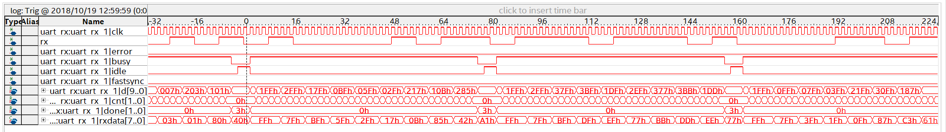
テストには、Zelaxのtestcomトラフィックジェネレーターが使用されました。 残念ながら、私のUSB / UARTアダプターは230400BPSを超える速度では動作しなかったため、すべてのテストはこの速度で実行されました。
多数決要素を使用して入力信号RXをフィルター処理したテスト結果 
信号タップ信号ステータス
信号タップ信号ステータス
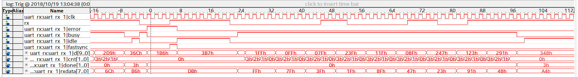
そしてここでは、多数の要素が入り口から取り除かれました。
しかし、高速同期スキームをチェックするときに、他にどのように任意のエラーをシミュレートできますか?

信号タップ信号ステータス
信号タップ信号ステータス
ご注意
申し訳ありませんが、Quartusのコースは受講しておらず、質問できる人はいませんでした。 自分がつまずいたこと、他のスタートアップFPGAについて警告すること:プロジェクトでSDCファイルを作成し、そのクロック周波数を記述してください。 はい、プロジェクトはそれなしでアセンブルされますが、シンセサイザがクロックの時間的特性を判断できなかった場合は警告が表示される場合があります。 最初は、コードを実行するときに受信モジュールでなぜ問題が発生するかを判断するために半日殺すまでそれらを無視しました
if(rx == 1'b0) begin busy <= 1'b1; d <= 10'b1111111111; cnt <= 2'd0; idle <= 1'b0; end else begin
ビジー信号とアイドル信号は正しく設定されましたが、レジスタdの内容は変更されない場合がありました。
付録:プロジェクトのSDCファイル
set_time_format -unit ns -decimal_places 3 # 50Mhz, (50/50 duty cycle) create_clock -name {clk50mhz} -period 20.000 -waveform { 0.000 10.000 } ############################################################################## Now that we have created the custom clocks which will be base clocks,# derive_pll_clock is used to calculate all remaining clocks for PLLs derive_pll_clocks -create_base_clocks derive_clock_uncertainty # PLL ? # altpll_component.clk0_divide_by = 15625, # altpll_component.clk0_duty_cycle = 50, # altpll_component.clk0_multiply_by = 576, # altpll_component.clk0_phase_shift = "0", #create_generated_clock -name clk_1843200 -source [get_ports {clk50mhz}] -divide_by 15625 -multiply_by 576 -duty_cycle 50 -phase 0 -offset 0 # baudrate=38400 # 1/4 , .. duty=(1/4)*100=25% #create_generated_clock -name uart_baud4 -source [get_nets {pll50mhz|altpll_component|auto_generated|wire_pll1_clk[0]}] -divide_by 12 -duty_cycle 25 [get_nets {uart_osc_1|LPM_COUNTER_component|auto_generated|counter_reg_bit[0]}] # baudrate=230400 # 1/4 , .. duty=(1/4)*100=50% create_generated_clock -name uart_baud4 -source [get_nets {pll50mhz|altpll_component|auto_generated|wire_pll1_clk[0]}] -divide_by 2 -duty_cycle 25 [get_nets {uart_osc_1|LPM_COUNTER_component|auto_generated|counter_reg_bit[0]}] # baudrate=460800 # 1, PLL, .
記事にコメントを書いてくれたすべての人に感謝します! これらのうち、私は多くの有用な情報を集めましたが、時々矛盾する情報もあります。 私の意見では、それらの値は上記のアルゴリズムの実装よりもはるかに大きいです。 そして、もちろん、それらはまた、FPGAの世界に入ることを敢えてする人々にとって有用です。
外部リンクのリスト