Boris Tsirlin and Alexander Kushnerov
10/30/2019
It is not difficult for an experienced circuit designer to find out a familiar circuit, no matter how it is drawn. In this article, we show that the two transistor circuits of the patents are a variant of the asynchronous counting trigger (AST). Compared to the standard circuit, some transistors are missing from the patents. This may be considered a malfunction. We will show that if the same fault occurs in the standard circuit, it continues to work correctly. An AST implemented only on OR-NOT elements [1] or only on AND-NOT elements is known as a Harvard trigger. Both variants of the schemes are shown in Fig. 1, where g7 is an indicator of transient completion. In the future, we will not consider it. In Fig. Figure 1 also shows the signal transition graphs (STGs) [2] built in Workcraft [3].
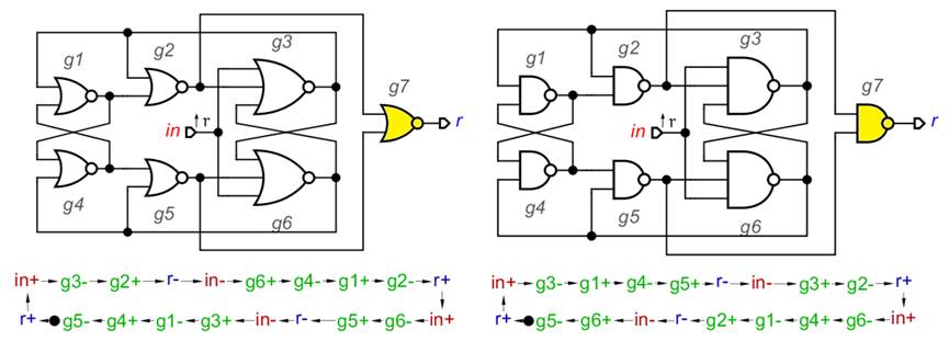
Fig. 1. Asynchronous counting trigger (AST) and its STG.
Note that in both versions of the AST there are three pairs of elements (g1, g2), (g4, g5) and (g3, g6) that have a common input. Transistor circuits of elements 2I-NOT and 2OR-NOT shown in Fig. 2. Three-input elements are arranged similarly and contain 6 transistors.
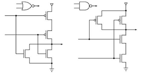
Fig. 2. Transistor circuits of elements 2I-NOT and 2OR-NOT.
We take two elements 2OR-NOT and select at each input, where the p-MOS transistor is connected to Upit. Connect these inputs together and connect to the ground (log. 0). Both transistors will open and the voltage at their drains will be equal to Upit. Is this enough to safely connect the drains and replace the two transistors with one, as shown in Fig. 3? Not. You need to check what happens if you log on the shared input. 1. The outputs of both elements will connect to the ground, and we will have a bridge circuit of four p-MOS transistors. For the remaining two inputs, we have four combinations 0 and 1. It is easy to show that in none of them there is a short circuit between Upit and ground.

Fig. 3. Two 2OR-NOT elements sharing a common input.
Let us now consider the pulse distributor circuit [4] in Fig. 4. Using Fig. 3, we can redraw this diagram as shown in Fig. 5. It is already possible to recognize AST in Fig. 1, however, there elements g3 and g6 have 3 inputs.

Fig. 4. The pulse distributor circuit from [4].
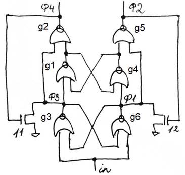
Fig. 5. A variant of the circuit in Fig. 4.
The gates of transistors 11 and 12 can be considered as inputs of elements 3OR-NOT, in which the third p-MOS transistor is shorted. Does this affect the correct operation of the circuit? Consider the order of appearance of the signals in, g2, and g6 at the input of the element g3. To do this, delete all other signals in the corresponding STG in Fig. 1 as shown in Fig. 6.

Fig. 6. STG for OR NOT. Signals in, g2, g6 and g3.
Since the third p-MOS transistor is shorted, g3 + switching can occur after switching in- and g6- (in any order) without allowing switching g2-. However, as can be seen from Fig. 6, in the section from g2 + to g2- there are only in- and g6 +, therefore, the forbidden switching g3 + does not occur. Before switching g2 +, the element g3 is already at 0, and at its input g6 is still 0, i.e. The first p-mos transistor is open. Switching g2 + opens transistor 11 and should turn off the shorted p-MOS transistor. This does not happen, moreover, switching in- opens the second p-MOS transistor. Thus, through two open p-MOS transistors and an open transistor 11, current begins to flow from Upit to ground. This continues for a short time until the next g6 + switch closes the first p-MOS transistor. During this time, transistor 11 provides 0 at the output of g3. How exactly? Suppose the resistances of open p-MOS and n-MOS transistors are the same and equal to R, then after switching in- the voltage on g3 jumps from 0 to (1/3) Upit, but this is in the ideal case. In practice, there is some parasitic capacitance between g3 and ground, the voltage at which increases smoothly and may not reach (1/3) Upit. One way or another, this voltage will be less than (1/2) Upit and means a log. 0. For transistor 12, everything is similar, it provides a short time 0 at the output of g6. Thus, the delays of the elements g6 and g3 determine two periods of time when the trigger consumes a large current of approximately equal to Upit / (3R).
Let us now consider the counting trigger circuit [5] in Fig. 7. Here, transistors 11, 12, 24, 23 form a 2I-NOT element, which, apparently, is an indicator of AST in Fig. 1. Another element 2I-NOT is formed by transistors 7, 13, 25 and 18. Let's pay attention to the fact that transistor 18 is connected to ground and similarly to the example in Fig. 3, is common to the three elements AND NOT. The second element 2I-NOT, which includes the transistor 18, is formed by transistors 5, 9, 21, and the third is 3I-NOT on the transistors 2, 4, 16, 20. In parallel with the transistors 2 and 4, there should be a third p-MOS transistor but he is absent. The circuit in Fig. 7 is symmetrical, for a better understanding we will redraw it as shown in Fig. 8.
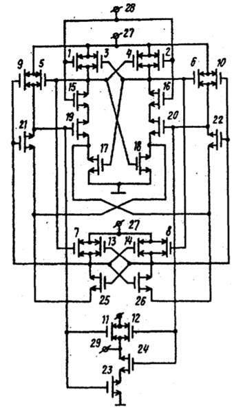
Fig. 7. Scheme of the countable trigger from [5].

Fig. 8. A variant of the circuit in Fig. 7.
Will there be outputs g3 and g6 in Fig. 8 switch correctly if the third p-mos transistor in parallel is missing? This will be understood after analyzing the STG in Fig. 9, which, as in the previous case, is obtained from the corresponding STG in Fig. 1 by removing all signals except in, g2, g6, and g3.
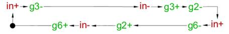
Fig. 9. STG for NAND. Signals in, g2, g6 and g3.
The g3 element is 3I-NOT, so after switching in +, g6 + and g2 + (in any order), g3- will switch. Any of the in-, g6-, or g2- reverse switchings should cause the g3 + switchover. However, g2- cannot open the missing p-MOS transistor, so g3 will remain at 0 and will wait for the in- or g6- to switch. As can be seen from Fig. 9, on the section from g3- to g3 + there is no switching g2- and the p-MOS transistor is not needed here. On the other hand, this transistor should provide a log. 1 to g3 when in and g6 switch arbitrarily. Consider in Fig. 9th section from g3 + to g2 +. Switching g2- closes transistor 19. Next, switching in + closes transistor 1 and opens transistor 15. Element g6 remains at 1, i.e. transistor 17 is open, and transistor 3 is closed. Thus, in + disconnects g3 from both the earth and Upit. However, the log is held on g3. 1, since in practice there is a parasitic capacitance between g3 and ground, which is charged up to Upit. Switching g6- opens transistor 3 and connects this capacitance to Upit. For the second half of the scheme, everything is similar. Thus, the delays of the elements g6 and g3 determine the time during which the state is stored on the tank. In practice, it is important that the leakage current of transistors 19 and 20 is small, otherwise the capacitance may discharge below (1/2) Upit in the allotted time.
Compared to standard AST in Fig. 1, in the diagrams in Fig. 5 and in Fig. 8, the function of setting 1 element of 3OR-NOT and the reset function of 0 element 3I-NOT damaged. This means that the standard AST will continue to work correctly, even if a corresponding malfunction occurs in elements g6 and g3. For a standard circuit (without g7), 28 transistors are needed. For circuits in Fig. 4 and in Fig. 7 (without transistors 11, 12, 24, 23) you need 23 and 22 transistors, respectively. If you return the missing p-MOS transistors, these circuits will work more reliably. The minimum number of transistors in the circuit in Fig. 7 does not necessarily mean that it is better than the circuit in Fig. 4 and better circuit in Fig. 1. In addition to the number of transistors and the current consumption, there are other important parameters, for example,
- complexity of an additional circuit for setting initial states
- load capacity (reload rate of load capacity)
- exit rate from metastable state
- number and values of parasitic capacitances
- number and values of leakage currents
A comparative analysis of these parameters, as well as a discussion of AST schemes implemented on other elements, is beyond the scope of this article.
Literature
[1] GT Osborne, "Asynchronous binary counter register stage with flip-flop and gate utilizing plurality of interconnected NOR circuits." Patent US3139540, 30 Jun. 1964.
[2] L. Ya. Rosenblum and A. V. Yakovlev, “On a new graphic form for illustrating the essence of the invention,” Issues of Invention, No. 11, pp. 36-40, 1988.
[3] https://workcraft.org
[4] V. I. Goryachev, B. M. Mansurov, Ya. D. Martynenko and R. G. Talibov, “Four-phase pulse distributor”. Copyright certificate SU342299, 06/14/1972.
[5] V. I. Varshavsky, N. M. Kravchenko, V. B. Marakhovsky and B. S. Tsirlin, “Counting trigger on CMOS transistors”. Copyright certificate SU1398069, 05.23.1988.