Why a heating pad, if there is a laptop: the study of thermal resistance at the atomic level

Many gamers around the world who have embarked on the Xbox 360 era are very familiar with the situation when their console turned into a pan on which to fry eggs. A similar sad situation is found not only with game consoles, but also with phones, laptops, tablets and much more. In principle, almost any electronics can experience heat stroke, which can lead not only to its breakdown and upset feelings of its owner, but also to the “bad boom” of the battery and serious injuries. Today we will meet with you a study in which scientists from Stanford University, like Nick Fury from the comics, created a shield that protects the heat-sensitive electronics from overheating and, as a result, prevents them from breaking. How did scientists manage to create a thermal shield, what are its main components and how effective is it? About this and not only we learn from the report of the research group. Go.
Study basis
The problem of overheating has been known for a very long time, and scientists solve it in a variety of ways. One of the most popular is the introduction of glass, plastic and even layers of air, which serve as a kind of insulators of thermal radiation. In modern realities, this method can be improved by reducing the thickness of the protective layer to several atoms without losing its thermal insulating properties. That is what the researchers did.
It is, of course, about nanomaterials. However, their use in thermal insulation was previously complicated by the fact that the wavelength of the coolants ( phonons * ) is much shorter than that of electrons or photons.
Phonon * is a quasiparticle, which is a quantum of vibrational motion of crystal atoms.In addition, due to the bosonic nature of phonons, it is impossible to control them by means of voltage (as is done with charge carriers), which generally complicates the control of heat transfer in solids.
Previously, the thermal properties of solids were controlled, as the researchers remind us, by means of nanolaminate films and superlattices due to structural disordering and high density of interfaces, or by silicon and germanium nanowires due to strong phonon scattering.
Scientists are ready to attribute to a number of the above methods of thermal insulation with two-dimensional materials, the thickness of which does not exceed several atoms, which makes it easy to control them on an atomic scale. In their study, they used the van der Waals (vdW) assembly of atomically thin 2D layers to achieve very high thermal resistance across their entire heterostructure.
Van der Waals forces * - forces of intermolecular / interatomic interaction with an energy of 10-20 kJ / mol.The new technique made it possible to obtain thermal resistance in a vdW heterostructure with a thickness of 2 nm, comparable with that in a layer of SiO 2 (silicon dioxide) with a thickness of 300 nm.
In addition, the use of vdW heterostructures made it possible to gain control over the thermal properties at the atomic level by layering heterogeneous two-dimensional monolayers with different atomic mass densities and vibrational modes.
So, we will not pull the cat by the mustache and proceed to consider the results of this amazing study.
Research results
First of all, we will get acquainted with the microstructural and optical characteristics of vdW heterostructures used in this study.

Image No. 1
Figure 1a shows a cross-sectional diagram of a four-layer heterostructure consisting of (top to bottom): graphene (Gr), MoSe 2 , MoS 2 , WSe2 2 and a SiO 2 / Si substrate. For simultaneous scanning of all layers, a Raman laser * with a wavelength of 532 nm is used.
Raman laser * is a type of laser in which Raman scattering is the main mechanism for amplifying light.Several methods were used to confirm the microstructural, thermal, and electrical uniformity of the heterostructures: scanning transmission electron microscopy (STEM), photoluminescent spectroscopy (PL), probe Kelvin microscopy (KPM), scanning thermal microscopy (SThM), and Raman spectroscopy and thermometry .
Raman scattering , in turn, is an inelastic scattering of optical radiation on the molecules of a substance, which is accompanied by a significant change in the radiation frequency.
Image 1b shows us the Raman spectrum of the Gr / MoSe 2 / MoS 2 / WSe2 2 heterostructure on a SiO 2 / Si substrate at the location indicated by the red dot. This graph shows the signature of each monolayer in the layer array, as well as the signature of the Si substrate.
1c - 1f shows dark-field STEM images of the Gr / MoSe 2 / MoS 2 / WSe2 2 heterostructure ( 1c ) and the Gr / MoS 2 / WSe2 2 ( 1d - 1f ) heterostructure with different lattice orientations. STEM images show atomically close vdW gaps without any contamination, which allows you to fully see the total thickness of these heterostructures. The presence of interlayer communication was also confirmed in large areas of scanning by means of photoluminescent (PL) spectroscopy ( 1g ). The photoluminescent signal of individual layers inside the heterostructure is significantly suppressed compared to the signal of an isolated monolayer. This is explained by the process of interlayer charge transfer due to the close interlayer interaction, which becomes even stronger after annealing.

Image No. 2
In order to measure the heat flux perpendicular to the atomic planes of the heterostructure, the array of layers was structured in the form of four-probe electrical devices. The top layer of graphene is in contact with palladium (Pd) electrodes and is used as a heater for Raman thermometry measurements.
This electrical heating method provides accurate quantification of input power. Another possible heating method, optical, would be more difficult to implement due to ignorance of the absorption coefficients of individual layers.
2a shows a four-probe measurement scheme, and 2b shows a top view of the test structure. Graph 2c shows the measured heat transfer characteristics for three devices, one of which contains only graphene, and two - arrays of Gr / WSe2 2 and Gr / MoSe 2 / WSe2 2 layers. All variants demonstrate the ambipolar behavior of graphene, which is associated with the absence of a forbidden zone.
It was also found that current conductivity and heating occur in the upper layer (in graphene), since its electrical conductivity is several orders of magnitude higher than that of MoS 2 and WSe2 2 .
To demonstrate the homogeneity of the tested devices, measurements were made using probe Kelvin microscopy (KPM) and scanning thermal microscopy (SThM). Graph 2d shows KPM measurements revealing a linear potential distribution. The results of SThM analysis are shown in 2e . Here we see a map of the electrically heated Gr / MoS 2 / WSe2 2 channels, as well as the presence of uniformity in surface heating.
The above-described scanning techniques, in particular SThM, confirmed the homogeneity of the investigated structure, that is, its homogeneity, in terms of temperature. The next step was the quantitative determination of the temperature of each of the component layers, performed using Raman spectroscopy (i.e., Raman spectroscopy).
All three devices were tested, the area of each of which was ~ 40 μm 2 . In this case, the heater power was changed by 9 mW, and the power of the absorbed laser was lower than ~ 5 μW with a laser spot area of ~ 0.5 μm 2 .

Image No. 3
Graph 3a shows an increase in temperature (∆T) of each layer and substrate as the heater power increases in the Gr / MoS 2 / WSe2 2 heterostructure.
The slopes of the linear function for each material (layer) indicate thermal resistance (R th = ∆T / P) between a single layer and a heat sink. Given the uniform distribution of heating over the area, the thermal resistance is quite simple to analyze from the lower to the upper layer, during which their values are normalized by the channel area (WL).
L and W are the length and width of the channel, which significantly exceed the thickness of the SiO 2 substrate and the lateral length of thermal heating, which is ~ 0.1 μm.
Therefore, we can derive the formula for the thermal resistance of the Si substrate, which will look like this:
R th, Si ≈ (WL) 1/2 / (2 k Si )
In this situation, k Si ≈ 90 W m – 1 K – 1 , which is the expected thermal conductivity of such a highly doped substrate.
The difference between R th, WSe 2 and R th, Si is the sum of the thermal resistance of SiO 2 with a thickness of 100 nm and the boundary thermal resistance (TBR) of the WSe 2 / SiO 2 interface.
Combining all the above aspects, it can be established that Rth, MoS 2 - Rth, WSe 2 = TBRMoS 2 / WSe 2 , and Rth, Gr - Rth, MoS 2 = TBRGr / MoS 2 . Therefore, TBR for each of the interfaces WSe 2 / SiO 2 , MoS 2 / WSe 2 and Gr / MoS 2 can be extracted from graph 3a .
Then, scientists compared the total thermal resistance of all heterostructures measured by Raman spectroscopy and thermal microscopy ( 3b ).
Two-layer and three-layer SiO 2 heterostructures showed effective thermal resistance in the range from 220 to 280 m 2 · K / GW at room temperature, which is equivalent to the thermal resistance of SiO 2 with a thickness of 290 to 360 nm. Despite the fact that the thickness of the studied heterostructures does not exceed 2 nm ( 1d - 1f ), their thermal conductivity is 0.007-0.009 W m – 1 K – 1 at room temperature.
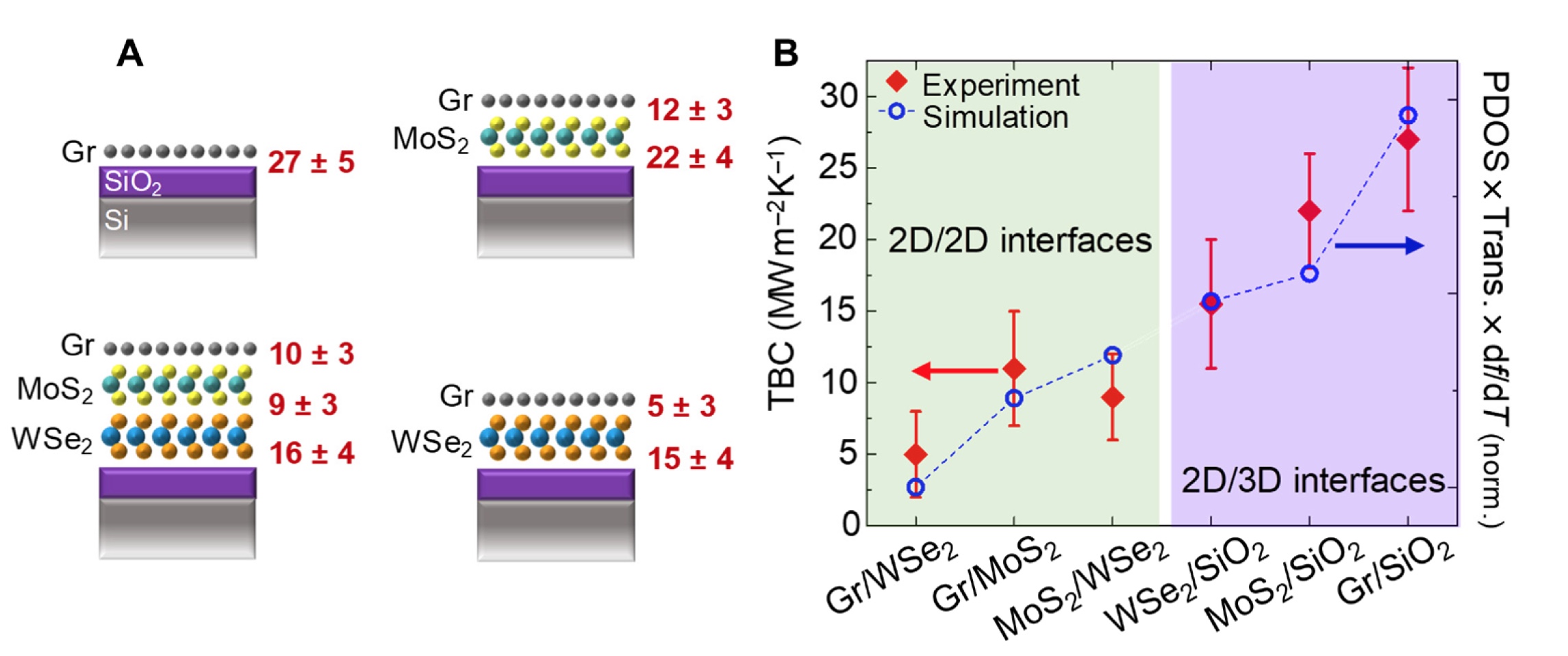
Image No. 4
Image 4 shows the results of measurements of all four structures and the boundary thermal conductivity (TBC) of their interfaces, which allows us to estimate the degree of influence of each layer on the previously measured thermal resistance (TBC = 1 / TBR).
Researchers note that this is the first-ever TBC measurement for atomically close interfaces between individual monolayers (2D / 2D), in particular between monolayers WSe 2 and SiO 2 .
The TBC of the WSe 2 / SiO 2 monolayer interface is lower than that of the WSe 2 / SiO 2 multilayer interface, which is not surprising, since the monolayer has significantly fewer bending phonon modes available for transmission. Simply put, the TBC interface between the 2D layer is lower than the TBC interface between the 2D layer and the 3D SiO 2 substrate ( 4b ).
For a more detailed acquaintance with the nuances of the study, I recommend that you look into the report of scientists and additional materials to it.
Epilogue
This study, according to the scientists themselves, gives us knowledge that can be applied in the implementation of atomic thermal interfaces. This work showed the possibility of creating heat-insulating metamaterials whose properties are not found in nature. In addition, the study also confirmed the possibility of making accurate temperature measurements of such structures, despite the atomic scale of the layers.
The heterostructures described above can become the basis of ultralight and compact thermal “shields”, which are able, for example, to remove heat from hot spots in electronics. In addition, this technology can be used in thermoelectric generators or in thermally controlled devices, increasing their productivity.
This study once again confirms that modern science is seriously carried away by the principle of "efficiency in a thimble", which can not be called a stupid undertaking, given the limited resources of the planet and the continuous increase in demand for all kinds of technological innovations.
Thank you for your attention, remain curious and have a good working week, guys! :)
Thank you for staying with us. Do you like our articles? Want to see more interesting materials? Support us by placing an order or recommending it to your friends, a 30% discount for Habr users on a unique analogue of entry-level servers that was invented by us for you: The whole truth about VPS (KVM) E5-2650 v4 (6 Cores) 10GB DDR4 240GB SSD 1Gbps from $ 20 or how to divide the server? (options are available with RAID1 and RAID10, up to 24 cores and up to 40GB DDR4).
Dell R730xd 2 times cheaper? Only we have 2 x Intel TetraDeca-Core Xeon 2x E5-2697v3 2.6GHz 14C 64GB DDR4 4x960GB SSD 1Gbps 100 TV from $ 199 in the Netherlands! Dell R420 - 2x E5-2430 2.2Ghz 6C 128GB DDR3 2x960GB SSD 1Gbps 100TB - from $ 99! Read about How to Build Infrastructure Bldg. class c using Dell R730xd E5-2650 v4 servers costing 9,000 euros for a penny?
All Articles