Apollo on-board control computer: dipstick and engineering analysis of memory on multiple stitched cores
Located on board the Apollo spacecraft, the control computer (Apollo Guidance Computer, AGC) helped the ship get to the moon and land on its surface. AGC software was physically woven into a read-only memory core core memory [core rope memory]. Ken Shirrif and like-minded people are rebuilding AGC (pictured below), which does not have enough memory on the cores, instead of which simulator boxes of such memory are installed. These boxes were used during program development and ground testing, so that engineers did not have to constantly flash memory. The simulator does not have documentation, so I [the author of the blog entry / approx. transl.] carried out its engineering analysis, assembled the interface, and using the simulator we launched programs on our AGC. However, in the process we encountered some difficulties.

AGC computer with cover removed. You can see the motherboard with a bunch of wires. In the places for memory, simulation boxes are visible. Interface cards in the foreground are modern.
The AGC contained six memory modules on multiple stitched cores, each of which stored only 6 kiloslovol of information (about 12 Kb). The memory modules were a bit like ROM cartridges for a video game, and they kept the software in a constant but erasable form. Programs were recorded by weaving wires through magnetic cores. The wire passing through the core denoted bit 1, and the bypassing one denoted bit 0. By weaving 192 wires through or around the core, it was possible to store 192 bits, which gave a much higher density than rewritable memory on magnetic cores, which stored one bit per core.
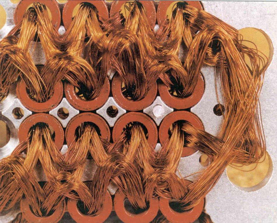
Memory on multiple stitched cores (Block I) with AGC
Making such a memory was a painstaking process that took 8 weeks and cost $ 15,000 per module. Experienced women passed the wires manually, stitching the cores one after another with a hollow needle through which the wire was threaded (pictured below). They were assisted by an automatic system that read the program from the punched tape and placed a hole above the core array. The weaver threaded the needle through the hole, leading the wire where needed. After that, the memory was mounted on the module along with hundreds of resistors and diodes, and was filled with epoxy for reliability in flight.
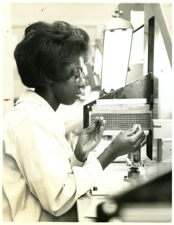
A woman flashes a permanent memory, introducing a program into it
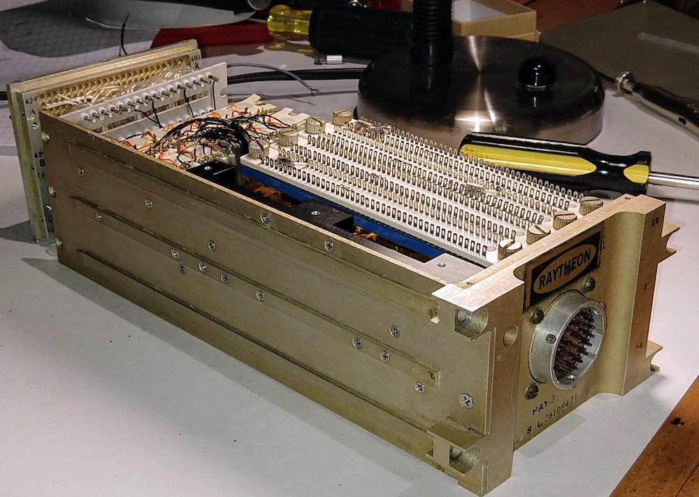
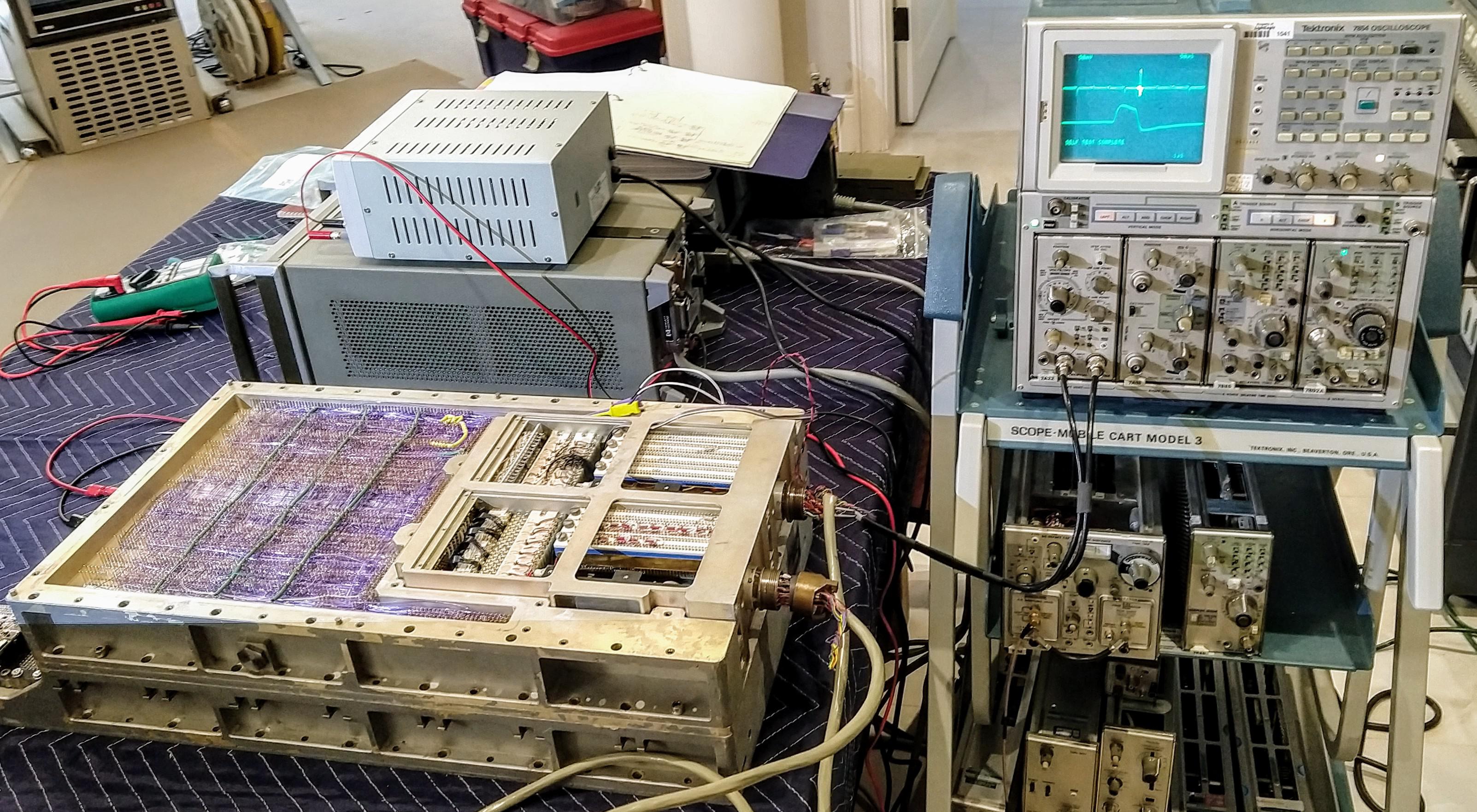
The process of flashing memory took a lot of time and money, so an alternative was required during testing and development. Instead of stitched cores, NASA used their simulators, allowing the AGC to download data from an external system. Our AGC was used for ground testing, so it did not have stitched cores, but had their simulator. It consists of two boxes connected to the connectors for stitched cores, and each box occupies three memory slots. They can be seen on the left side of the AGC in the photo below, and they have round military connectors for connecting to an external computer.

Simulator boxes are installed on the left side of the AGC instead of real memory modules.
Although we have detailed documentation for the AGC, I could not find the documentation for the simulator. I had to apply engineering analysis, following all the schemes and realizing what the boxes do. External study of them gives little. On one side of each box there is a MIL-Spec connector for connecting to an external system. On the other hand, there are three groups of 96 pins connected to the AGC. Each group of contacts takes the place of one memory module on the cores.

Opening the boxes showed non-standard assembly techniques. Partially in the contours, a method was used that was structurally similar to cordwood - the components were mounted vertically with holes in the metal block. On both sides of the unit, the contacts were soldered to the wires. Other circuits in the boxes used standard integrated circuits (TTL 7400). But unlike modern printed circuit boards, the chips were mounted inside plastic modules called “dipstik” [ Dipstik, eng. - probe ] and were wound together with wires.
The “cordwood” layout was actively used in the AGC to create analog circuits, and it is also present in memory simulators (see photo below). The white circles in the center are the ends of the resistors and diodes mounted vertically in the module and with the contacts soldered on both sides. The components are densely packed, like logs, which is why this layout is called cordwood. Pulse transformers are located under large gray circles. There are the same ones on the other side of the module, and their orange, yellow, red and brown wires come out of the holes. Black wires connect the cordwood circuitry to digital logic. At the top of the photo you can see the pegs on which the diodes and resistors are mounted, together with the connection with the contacts connected to the AGC.

The main goal of the Cordwood layout is to provide electrical isolation between AGC circuits and memory simulator boxes. In modern circuits, optoisolators perform this function, but simulators used small pulse transformers instead. Since each box receives signals designed for three different memory modules, many diodes combine three signals into one. Resistors control the current passing through pulse transformers.
Understanding the structure of analog cordwood circuits was difficult. Firstly, the component is not visible, since they are integrated into the module. I had to use a multimeter to understand where they are. Secondly, since in the layout of the cordwood contacts appear on both sides, I spent a lot of time turning the box over in search of the necessary contacts. Finally, I could not come up with a convenient way to draw a layout diagram of a cordwood that did not generate a maze of lines.
Dipstik was a plug-in introduced in 1968 to facilitate prototyping of integrated circuits. He replaced circuit boards with a double density packaging system.
The idea was in the plastic block of the connector with the connection of the wrap contacts from the bottom to connect the circuit. Integrated circuits were mounted on a holder inserted into the connector block. The holder on top had soldering ears for installing additional components, such as decoupling capacitors. The photo below shows dipstick modules with one holder pulled out. Each holder housed 5 IPs. The contacts of the IC were placed between the contacts of the holder and the contacts of the connector block. This idea seemed good, but in the end it was unreliable. Deepstick was a failed project.

The photo below shows the contacts connected with the help of wire wrapping from the bottom of the dipsticks. It was extremely difficult for me to track them, it was impossible to go through each posting in the sea of identical blue wires. I had to ring everything with a multimeter. Then I was able to draw a schematic diagram and think about what it does. In total, about 50 ICs were used in the simulator.

Judging by the labeling of the components, the simulator boxes were assembled in 1971. And although only a few years passed since the design of AGC, the technologies in the simulators already look more advanced, which illustrates the rapid progress of IP from the mid-1960s to the early 1970s. AGC was assembled on the basis of simple integrated circuits, each of which contains two NOR valves and a primitive resistor-transistor logic (RTL) is built in. In the boxes of simulators there are already more complex chips of the 7400th series, containing more than ten elements on transistor-transistor logic (TTL). Unlike obsolete flat ICs in AGC, simulator boxes use chips in the DIP (dual in-line package) package, and such cases are still in use.
Having tracked all the contours, I realized how the simulator works, and drew the diagrams . In fact, one box decodes the address from which access is being accessed, and the second sends the necessary data to the AGC (I will call it the “address box” and “data box”).
The address box receives the signals and converts them to binary. The task is not simple, because the signals come in the form of high current pulses and 14 V voltage, which are designed to switch cores. Also, these pulses are separated in time, as some switch the core in one direction, while others switch back. Finally, the pulses sent to the cores contain not only an address, but also a signal to select one of the 6 modules, and to select one of the 12 threads in the module.
The address box uses pulse converters, converting 14 V pulses into TTL signals. It contains a bunch of AND-OR logic for converting signals to binary addresses (and this is not trivial, since each module contains 6 kiloslovol, this is not a power of two, so many bitwise manipulations are required). A flip flop blocks an address when one is available. Finally, the RC circuit of the multivibrator controls the timing, determining on the basis of various signals the availability of the address, and when to send the result to the AGC.
The data box is simpler. It receives 16 bits of data from an external system and sends signals to AGC amplifiers, simulating millivolt signals from the core. These signals are generated by pulse converters. The address box and data box communicate through the wires of the AGC backplane.
Boxes communicate with an external system using differential signals to eliminate noise from long cables. The boxes contain 5 V LM109 regulators supplying TTLs. One box receives an unregulated DC through an external connector and sends an unregulated DC to another through an AGC backplane (which, to me, is rather strange).

Having dealt with the work of the simulator, then it was necessary to create an interface capable of delivering data from the program to the simulator. I used BeagleBone , a tiny Linux-based single-board computer. The advantage of BeagleBone is that it has fast microcontrollers that can respond in real time to memory requests from AGC.
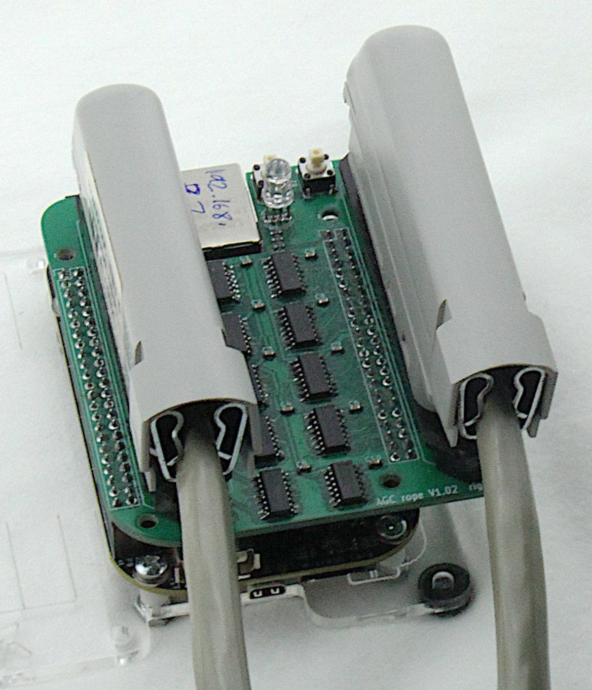
The interface is the board stuck in the BeagleBone. Each of the two cables goes to its box simulator.
I designed an interface board for connecting to a BeagleBone. It is quite simple: AM26C32 differential linear receivers that convert the differential signals of the simulator to 3.3 V logic signals for BeagleBone, and AM26C31 differential linear drivers for sending signals to the simulator. I designed the board at KiCad and ordered production from PCBWay , the sponsor of the restoration of AGC.
I wrote a program that runs on a BeagleBone microcontroller, PRU. This is, in fact, a state machine, waiting for the address from the simulator box, waiting for the timing signal, reading the word from BeagleBone RAM, and sending the word to the simulator. I posted the program on Github .
Memory simulators on repeatedly stitched cores were not assembled according to the Apollo on-board control computer standards, and as a result, I had to spend a lot of time debugging them. Many connections were broken, they had to be re-soldered again (I don’t know if they broke from time to time, or when I understood the working scheme). We also found a short circuit in one dipstick and a faulty IC.
Most of all the problems were with dipsticks, since many contacts interspersed between dipsticks and IP. The problem was that the contacts of the IC were located in the manner of a sandwich between the contacts on the dipstick holder and the block where they were inserted. Plastic dipsticks bend outward, which is why the contacts periodically do not work. Having bent the legs of the IP in the form of the letter S, Mark managed to provide them with contact from both sides, at least for a while. But after a few hours, the soft legs of the IC bent back, the contacts began to work badly again, so we did not have a long-term solution to this problem.
The most interesting problem was the race of two signals from the AGC, which were supposed to stop simultaneously. They fed both ends of the coil of the pulse converter, which was not supposed to give a signal. However, one signal lagged behind the other, which led to the appearance of a spurious impulse. Unfortunately, the digital logic in the simulator box was asynchronous, this impulse blocked the wrong bit of the address in the flip flops, and as a result, access to the wrong place in the memory occurred. As a result, we tracked this problem and installed additional capacitors that filter the pulse. Unfortunately, we took too large capacitors and the signal in other cases was delayed too much, which led to the appearance of other errors. Then we put smaller capacitors, and finally managed to successfully run programs on AGC using vintage core memory simulators.
The Apollo on-board control computer uses memory on multiple stitched cores. Since it would be impractical to constantly remake such a memory during development, simulators were used instead. I carried out an engineering analysis of the simulator and created an interface for its operation using BeagleBone. We have successfully launched AGC programs through this interface. However, the memory simulator turned out to be problematic and unreliable.
@CuriousMarc made a video detailing our work with the memory simulator:
AGC computer with cover removed. You can see the motherboard with a bunch of wires. In the places for memory, simulation boxes are visible. Interface cards in the foreground are modern.
Multi-stitched memory
The AGC contained six memory modules on multiple stitched cores, each of which stored only 6 kiloslovol of information (about 12 Kb). The memory modules were a bit like ROM cartridges for a video game, and they kept the software in a constant but erasable form. Programs were recorded by weaving wires through magnetic cores. The wire passing through the core denoted bit 1, and the bypassing one denoted bit 0. By weaving 192 wires through or around the core, it was possible to store 192 bits, which gave a much higher density than rewritable memory on magnetic cores, which stored one bit per core.
Memory on multiple stitched cores (Block I) with AGC
Making such a memory was a painstaking process that took 8 weeks and cost $ 15,000 per module. Experienced women passed the wires manually, stitching the cores one after another with a hollow needle through which the wire was threaded (pictured below). They were assisted by an automatic system that read the program from the punched tape and placed a hole above the core array. The weaver threaded the needle through the hole, leading the wire where needed. After that, the memory was mounted on the module along with hundreds of resistors and diodes, and was filled with epoxy for reliability in flight.
A woman flashes a permanent memory, introducing a program into it
Simulator of memory on repeatedly stitched cores
The process of flashing memory took a lot of time and money, so an alternative was required during testing and development. Instead of stitched cores, NASA used their simulators, allowing the AGC to download data from an external system. Our AGC was used for ground testing, so it did not have stitched cores, but had their simulator. It consists of two boxes connected to the connectors for stitched cores, and each box occupies three memory slots. They can be seen on the left side of the AGC in the photo below, and they have round military connectors for connecting to an external computer.
Simulator boxes are installed on the left side of the AGC instead of real memory modules.
Although we have detailed documentation for the AGC, I could not find the documentation for the simulator. I had to apply engineering analysis, following all the schemes and realizing what the boxes do. External study of them gives little. On one side of each box there is a MIL-Spec connector for connecting to an external system. On the other hand, there are three groups of 96 pins connected to the AGC. Each group of contacts takes the place of one memory module on the cores.
Opening the boxes showed non-standard assembly techniques. Partially in the contours, a method was used that was structurally similar to cordwood - the components were mounted vertically with holes in the metal block. On both sides of the unit, the contacts were soldered to the wires. Other circuits in the boxes used standard integrated circuits (TTL 7400). But unlike modern printed circuit boards, the chips were mounted inside plastic modules called “dipstik” [ Dipstik, eng. - probe ] and were wound together with wires.
Cordwood layout
The “cordwood” layout was actively used in the AGC to create analog circuits, and it is also present in memory simulators (see photo below). The white circles in the center are the ends of the resistors and diodes mounted vertically in the module and with the contacts soldered on both sides. The components are densely packed, like logs, which is why this layout is called cordwood. Pulse transformers are located under large gray circles. There are the same ones on the other side of the module, and their orange, yellow, red and brown wires come out of the holes. Black wires connect the cordwood circuitry to digital logic. At the top of the photo you can see the pegs on which the diodes and resistors are mounted, together with the connection with the contacts connected to the AGC.
The main goal of the Cordwood layout is to provide electrical isolation between AGC circuits and memory simulator boxes. In modern circuits, optoisolators perform this function, but simulators used small pulse transformers instead. Since each box receives signals designed for three different memory modules, many diodes combine three signals into one. Resistors control the current passing through pulse transformers.
Understanding the structure of analog cordwood circuits was difficult. Firstly, the component is not visible, since they are integrated into the module. I had to use a multimeter to understand where they are. Secondly, since in the layout of the cordwood contacts appear on both sides, I spent a lot of time turning the box over in search of the necessary contacts. Finally, I could not come up with a convenient way to draw a layout diagram of a cordwood that did not generate a maze of lines.
Digital logic and dipstick
Dipstik was a plug-in introduced in 1968 to facilitate prototyping of integrated circuits. He replaced circuit boards with a double density packaging system.
The idea was in the plastic block of the connector with the connection of the wrap contacts from the bottom to connect the circuit. Integrated circuits were mounted on a holder inserted into the connector block. The holder on top had soldering ears for installing additional components, such as decoupling capacitors. The photo below shows dipstick modules with one holder pulled out. Each holder housed 5 IPs. The contacts of the IC were placed between the contacts of the holder and the contacts of the connector block. This idea seemed good, but in the end it was unreliable. Deepstick was a failed project.
The photo below shows the contacts connected with the help of wire wrapping from the bottom of the dipsticks. It was extremely difficult for me to track them, it was impossible to go through each posting in the sea of identical blue wires. I had to ring everything with a multimeter. Then I was able to draw a schematic diagram and think about what it does. In total, about 50 ICs were used in the simulator.
Judging by the labeling of the components, the simulator boxes were assembled in 1971. And although only a few years passed since the design of AGC, the technologies in the simulators already look more advanced, which illustrates the rapid progress of IP from the mid-1960s to the early 1970s. AGC was assembled on the basis of simple integrated circuits, each of which contains two NOR valves and a primitive resistor-transistor logic (RTL) is built in. In the boxes of simulators there are already more complex chips of the 7400th series, containing more than ten elements on transistor-transistor logic (TTL). Unlike obsolete flat ICs in AGC, simulator boxes use chips in the DIP (dual in-line package) package, and such cases are still in use.
Engineering Analysis Results
Having tracked all the contours, I realized how the simulator works, and drew the diagrams . In fact, one box decodes the address from which access is being accessed, and the second sends the necessary data to the AGC (I will call it the “address box” and “data box”).
The address box receives the signals and converts them to binary. The task is not simple, because the signals come in the form of high current pulses and 14 V voltage, which are designed to switch cores. Also, these pulses are separated in time, as some switch the core in one direction, while others switch back. Finally, the pulses sent to the cores contain not only an address, but also a signal to select one of the 6 modules, and to select one of the 12 threads in the module.
The address box uses pulse converters, converting 14 V pulses into TTL signals. It contains a bunch of AND-OR logic for converting signals to binary addresses (and this is not trivial, since each module contains 6 kiloslovol, this is not a power of two, so many bitwise manipulations are required). A flip flop blocks an address when one is available. Finally, the RC circuit of the multivibrator controls the timing, determining on the basis of various signals the availability of the address, and when to send the result to the AGC.
The data box is simpler. It receives 16 bits of data from an external system and sends signals to AGC amplifiers, simulating millivolt signals from the core. These signals are generated by pulse converters. The address box and data box communicate through the wires of the AGC backplane.
Boxes communicate with an external system using differential signals to eliminate noise from long cables. The boxes contain 5 V LM109 regulators supplying TTLs. One box receives an unregulated DC through an external connector and sends an unregulated DC to another through an AGC backplane (which, to me, is rather strange).
BeagleBone as an interface
Having dealt with the work of the simulator, then it was necessary to create an interface capable of delivering data from the program to the simulator. I used BeagleBone , a tiny Linux-based single-board computer. The advantage of BeagleBone is that it has fast microcontrollers that can respond in real time to memory requests from AGC.
The interface is the board stuck in the BeagleBone. Each of the two cables goes to its box simulator.
I designed an interface board for connecting to a BeagleBone. It is quite simple: AM26C32 differential linear receivers that convert the differential signals of the simulator to 3.3 V logic signals for BeagleBone, and AM26C31 differential linear drivers for sending signals to the simulator. I designed the board at KiCad and ordered production from PCBWay , the sponsor of the restoration of AGC.
I wrote a program that runs on a BeagleBone microcontroller, PRU. This is, in fact, a state machine, waiting for the address from the simulator box, waiting for the timing signal, reading the word from BeagleBone RAM, and sending the word to the simulator. I posted the program on Github .
Simulator issues
Memory simulators on repeatedly stitched cores were not assembled according to the Apollo on-board control computer standards, and as a result, I had to spend a lot of time debugging them. Many connections were broken, they had to be re-soldered again (I don’t know if they broke from time to time, or when I understood the working scheme). We also found a short circuit in one dipstick and a faulty IC.
Most of all the problems were with dipsticks, since many contacts interspersed between dipsticks and IP. The problem was that the contacts of the IC were located in the manner of a sandwich between the contacts on the dipstick holder and the block where they were inserted. Plastic dipsticks bend outward, which is why the contacts periodically do not work. Having bent the legs of the IP in the form of the letter S, Mark managed to provide them with contact from both sides, at least for a while. But after a few hours, the soft legs of the IC bent back, the contacts began to work badly again, so we did not have a long-term solution to this problem.
The most interesting problem was the race of two signals from the AGC, which were supposed to stop simultaneously. They fed both ends of the coil of the pulse converter, which was not supposed to give a signal. However, one signal lagged behind the other, which led to the appearance of a spurious impulse. Unfortunately, the digital logic in the simulator box was asynchronous, this impulse blocked the wrong bit of the address in the flip flops, and as a result, access to the wrong place in the memory occurred. As a result, we tracked this problem and installed additional capacitors that filter the pulse. Unfortunately, we took too large capacitors and the signal in other cases was delayed too much, which led to the appearance of other errors. Then we put smaller capacitors, and finally managed to successfully run programs on AGC using vintage core memory simulators.
Conclusion
The Apollo on-board control computer uses memory on multiple stitched cores. Since it would be impractical to constantly remake such a memory during development, simulators were used instead. I carried out an engineering analysis of the simulator and created an interface for its operation using BeagleBone. We have successfully launched AGC programs through this interface. However, the memory simulator turned out to be problematic and unreliable.
@CuriousMarc made a video detailing our work with the memory simulator:
All Articles