How to catch electrons: timeline development of electron microscopy
This article is a continuation of a series of materials about an electron microscope in a garage. Just in case, here is a link to the first issue .
Our project approached that stage when a detector is needed (electrons, secondary or elastically reflected). But before I tell you, why this particular detector is needed and how scientists came to its modern design.
For clarity, we will do this in the form of a timeline.
Considering the propagation of light as a wave process, Ernst Abbe was upset by the impossibility of overcoming the diffraction limit at that time. “It remains only to be comforted by the fact that the human genius will someday find ways and means to overcome this limit ...” [1]
At this point, scientists realized that the wavelength of the electron beam was so small that it would allow a microscope to be constructed that was significantly superior to an optical microscope.
This year, Max Knoll (and Ernst Ruska) for the first time received an image by scanning the sample surface with an electron beam. There was no additional system for focusing the electron beam, so the smallest beam diameter that could be obtained was 100 µm.
[2]
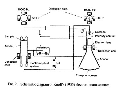
Figure from [3].
The beam current was measured by micro amperes, so it was possible to amplify the signal from the conductive sample with the help of electron tubes already then developed. This is how the absorbed current detector (absorbed current / specimen current) appeared.
In fact, Knoll got this image in secondary electrons. Because the current absorbed by the sample is how many electrons hit it (the scanning beam) minus those that flew off or were emitted again.
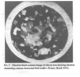
The magnification varied from 1x to 10x by changing the amplitude of oscillations of the electron beam in the microscope (which, by the way, was demonstrated earlier by V. Zvorykin in an optical microscope equipped with a television camera). To obtain a larger increase, you need to reduce the diameter of the beam.
Image of ferrosilicon from [3].
Developed modern electrostatic photomultipliers , then for short - PMT . The development of a photomultiplier in the United States was conducted by RCA, in which V. Zvorykin also worked on an electron microscope.
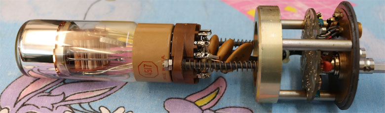
Example of PMT with connected electronics. The same photomultiplier produced by RCA, type 4517.
The PMT is a very sensitive device suitable for registering individual photons. Its gain is about 100 million.
The principle of operation is very simple. Through the entrance window of quartz glass photons fall on the photocathode.

The photocathode emits electrons that fly to special electrodes - dynodes arranged in series. The secondary emission coefficient of dinodes is greater than one: one electron has flown in, and more than one has flown out. Thus, an avalanche-like increase in the number of electrons is obtained, which at the end reach the anode, from which the useful signal is taken. The potential difference between the dinodes is maintained by means of a resistive divider; therefore, the PMT is called electrostatic.
In this PMT, the dynods are arranged nonlinearly:

Manfred von Ardenne used already open electrostatic and electromagnetic lenses (in the figure above, they are shown to focus the beam in a cathode ray tube) to reduce the diameter of the electron beam up to 4 nm.
But the beam current has become so small ( A, i.e. about 0.1 pA), which was not possible to amplify it with a warm tube amplifier: the useful signal was much less noise.
I had to record the resulting image on the light (or reflection) on the film, with an exposure time of about 20 minutes. To focus, there was a separate system with a solid zinc sulfide crystal, examined with an optical microscope.
At the same time, Vladimir Zvorykin worked on an electron microscope. He designed a scanning electron microscope in its modern sense: an electron-optical column, a sample chamber, a vacuum system. Scanning standard on TV at the time in the USA: 441 lines, 30 fps. But as the beam diameter decreased to less than 1 micron, the current became too small and as a result of the amplification there was only noise.
The next attempt was to increase the beam current and apply a cathode with field emission. For this, we again had to return to the sealed glass tube, forgetting about the change of samples. But it was possible to experimentally get an increase of 8000x.
Returning again to a scanning electron microscope with a disconnected vacuum system, Vladimir Kozmich proposed the following solution:
Position the luminescent screen next to the sample, and then detect photons emitted by it using a photomultiplier (the photomultiplier was developed by the same company that Zvorykin worked for).
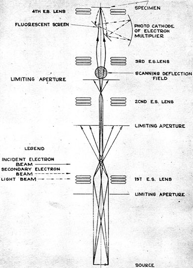
Figure from [4].
The advantage of this double-conversion solution (electrons - photons - electrons) is that you can reduce the scanning speed and thus increase the signal-to-noise ratio to the required.
From here came the slow scan mode, which is also available in modern electron microscopes. But because of this mode, the image was no longer displayed in real time, but was recorded with a special fax machine (apparently, produced by the same company). And again the same problem arises with adjusting the focus, but the solution suggested von Ardenne even earlier: by observing one scan line on an oscilloscope, adjust the focus so that high frequencies prevail.
Interestingly, the sample had a potential of + 800V, the cathode was grounded, and the electrons were accelerated by the anode to 10 keV. Thus, electrons hit the luminescent screen with an energy of 9.2 keV. It was necessary for the work of the fourth, immersion electrostatic lens, which was supposed to affect only the secondary electrons, and not the original beam.
Palluel published a paper in which he experimentally showed the dependence of the emission of elastically reflected electrons on the atomic number of an element for an electron beam with an energy of 20 keV. The larger the number, the greater the emission of electrons. This was a fairly important discovery, but it was not until 1957 that the first image with the contrast in atomic number was obtained.
At present, with the development of semiconductor detectors of reflected electrons, it is not difficult to obtain such a contrast. For example, a photo from the past video about gallium antimonide:
Even with an accelerating voltage of 15kV, the compositional contrast is strongly noticeable.
Thomas Everhart and Richard Thornley have developed an improved version of the electron detector, which is named after them: Everhart-Thornley Detector. This is the most common detector used in scanning electron microscopes to this day. In fact, the principle itself has remained unchanged since 1942. Novelty was added to the detection of elastically reflected electrons, where semiconductor sensors are widely used.
What did Everhart and Thornley offer? Schematically it looks like this:
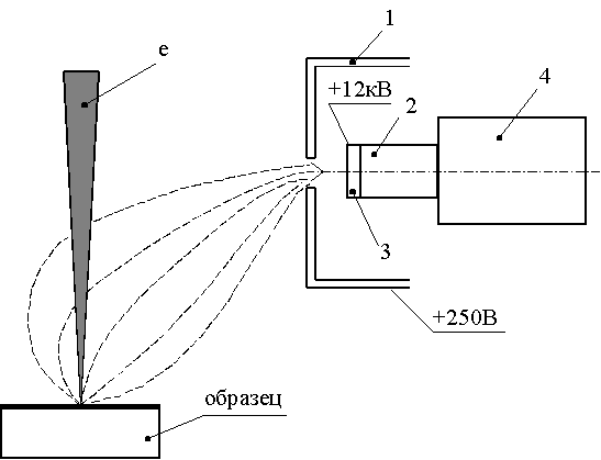
Figure from [5].
In the vacuum chamber of the microscope, next to the sample is a Faraday cage 1. Inside it is a luminescent screen 3 ( scintillator ), which emits photons when electrons hit it. These photons through fiber 2 go beyond the vacuum chamber and enter the photomultiplier, where they are converted back into electrons at the photocathode and amplified many times due to the emission of secondary electrons on the dinodes inside the photomultiplier.
In order not to make an immersion lens, like Zvorykin, and not to keep an object table at 800 V potential, the Faraday 1 cell performs the function of a collector: a positive potential of about 200-400 V is applied to it, which attracts secondary electrons with low energies but little effect on the main electron beam.
But electrons with energies of the order of hundreds of eV will not lead to the excitation of the phosphor and the emission of a sufficient number of photons. Therefore, the scintillator 3 (if it is metallized, if not, you have to make an electrostatic lens around it), an accelerating voltage of about 12kV is applied, which is guaranteed to excite the phosphor. By the way, if there were no Faraday 1 cell, then this voltage would have a significant impact on the main beam, strongly rejecting it.
Metallized scintillator.
It would seem that a lot of unnecessary transformations, but "it just works."
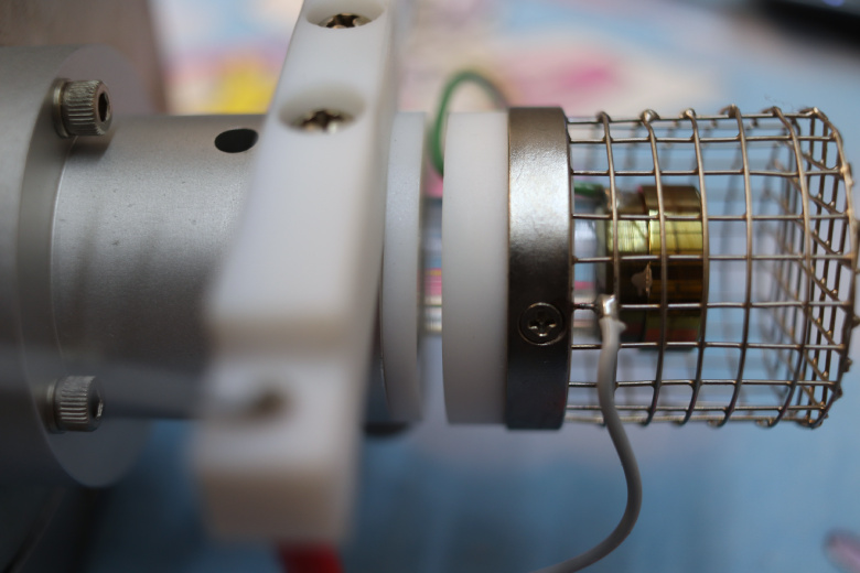
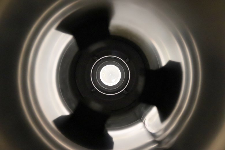
At the beginning of the article, I took a photograph of the vacuum part of the Everhart-Thornley detector, where one can visually see the Faraday cage, the metallized scintillator, the wires that supply accelerating voltage, and so on.
And this is how the photomultiplier tube seesthe scintillator world around :
Now you can make your own Everhart-Thornley detector for our JEOL, an absorbed current amplifier, and try to make a semiconductor detector of reflected electrons.
One year has passed since the first publication. During this time, I managed to learn a lot, in many ways to figure it out, and share it with you. Meet with very interesting people who have greatly helped the project. And, write ten articles about the electron microscope in the garage.
Of course, I wanted to bring the project to the first image to this date, but was very busy. Nevertheless, on the way new articles about electronics, experiments with an electron beam and a lot more - I hope you like it! Immediately after the release of each article, I check the comments every few minutes, who writes what, whether they approve, whether there are any inaccuracies that need correction. Throughout the year, this feedback is the main motivation to continue working on the project.
Happy New Year!
1. P.Hoks. Electron optics and electron microscopy. Moscow 1974.
2. THE SCANNING ELECTRON MICROSCOPE. A Small World of Huge Possibilities.
3. SCANNING ELECTRON MICROSCOPY 1928–1965. D. McMullan, Cavendish Laboratory, University of Cambridge, UK.
4. www.rfcafe.com/references/radio-craft/scanning-electron-microscope-september-1942-radio-craft.htm
5. Bykov Yu.A., Karpukhin S.D. Scanning electron microscopy and X-ray microanalysis. Tutorial. MGTU them. N.E. Bauman.
Our project approached that stage when a detector is needed (electrons, secondary or elastically reflected). But before I tell you, why this particular detector is needed and how scientists came to its modern design.
For clarity, we will do this in the form of a timeline.
1873 - 1878
Considering the propagation of light as a wave process, Ernst Abbe was upset by the impossibility of overcoming the diffraction limit at that time. “It remains only to be comforted by the fact that the human genius will someday find ways and means to overcome this limit ...” [1]
1935
At this point, scientists realized that the wavelength of the electron beam was so small that it would allow a microscope to be constructed that was significantly superior to an optical microscope.
This year, Max Knoll (and Ernst Ruska) for the first time received an image by scanning the sample surface with an electron beam. There was no additional system for focusing the electron beam, so the smallest beam diameter that could be obtained was 100 µm.
[2]
Figure from [3].
The beam current was measured by micro amperes, so it was possible to amplify the signal from the conductive sample with the help of electron tubes already then developed. This is how the absorbed current detector (absorbed current / specimen current) appeared.
In fact, Knoll got this image in secondary electrons. Because the current absorbed by the sample is how many electrons hit it (the scanning beam) minus those that flew off or were emitted again.
The magnification varied from 1x to 10x by changing the amplitude of oscillations of the electron beam in the microscope (which, by the way, was demonstrated earlier by V. Zvorykin in an optical microscope equipped with a television camera). To obtain a larger increase, you need to reduce the diameter of the beam.
Image of ferrosilicon from [3].
Difference from light microscopy
Hence the diametrical opposite of light and electron microscopy: if in a light one needs to enlarge the image of the sample (translucent or reflected), then in the electronic one it is necessary to reduce the image of the radiation source as much as possible. The exception is made only by transmission electron microscopes, but I already wrote about this.
1937
Developed modern electrostatic photomultipliers , then for short - PMT . The development of a photomultiplier in the United States was conducted by RCA, in which V. Zvorykin also worked on an electron microscope.
Example of PMT with connected electronics. The same photomultiplier produced by RCA, type 4517.
The PMT is a very sensitive device suitable for registering individual photons. Its gain is about 100 million.
The principle of operation is very simple. Through the entrance window of quartz glass photons fall on the photocathode.
The photocathode emits electrons that fly to special electrodes - dynodes arranged in series. The secondary emission coefficient of dinodes is greater than one: one electron has flown in, and more than one has flown out. Thus, an avalanche-like increase in the number of electrons is obtained, which at the end reach the anode, from which the useful signal is taken. The potential difference between the dinodes is maintained by means of a resistive divider; therefore, the PMT is called electrostatic.
In this PMT, the dynods are arranged nonlinearly:
1938
Manfred von Ardenne used already open electrostatic and electromagnetic lenses (in the figure above, they are shown to focus the beam in a cathode ray tube) to reduce the diameter of the electron beam up to 4 nm.
But the beam current has become so small ( A, i.e. about 0.1 pA), which was not possible to amplify it with a warm tube amplifier: the useful signal was much less noise.
I had to record the resulting image on the light (or reflection) on the film, with an exposure time of about 20 minutes. To focus, there was a separate system with a solid zinc sulfide crystal, examined with an optical microscope.
1942
At the same time, Vladimir Zvorykin worked on an electron microscope. He designed a scanning electron microscope in its modern sense: an electron-optical column, a sample chamber, a vacuum system. Scanning standard on TV at the time in the USA: 441 lines, 30 fps. But as the beam diameter decreased to less than 1 micron, the current became too small and as a result of the amplification there was only noise.
The next attempt was to increase the beam current and apply a cathode with field emission. For this, we again had to return to the sealed glass tube, forgetting about the change of samples. But it was possible to experimentally get an increase of 8000x.
Returning again to a scanning electron microscope with a disconnected vacuum system, Vladimir Kozmich proposed the following solution:
Position the luminescent screen next to the sample, and then detect photons emitted by it using a photomultiplier (the photomultiplier was developed by the same company that Zvorykin worked for).
Figure from [4].
The advantage of this double-conversion solution (electrons - photons - electrons) is that you can reduce the scanning speed and thus increase the signal-to-noise ratio to the required.
From here came the slow scan mode, which is also available in modern electron microscopes. But because of this mode, the image was no longer displayed in real time, but was recorded with a special fax machine (apparently, produced by the same company). And again the same problem arises with adjusting the focus, but the solution suggested von Ardenne even earlier: by observing one scan line on an oscilloscope, adjust the focus so that high frequencies prevail.
Interestingly, the sample had a potential of + 800V, the cathode was grounded, and the electrons were accelerated by the anode to 10 keV. Thus, electrons hit the luminescent screen with an energy of 9.2 keV. It was necessary for the work of the fourth, immersion electrostatic lens, which was supposed to affect only the secondary electrons, and not the original beam.
1947
Palluel published a paper in which he experimentally showed the dependence of the emission of elastically reflected electrons on the atomic number of an element for an electron beam with an energy of 20 keV. The larger the number, the greater the emission of electrons. This was a fairly important discovery, but it was not until 1957 that the first image with the contrast in atomic number was obtained.
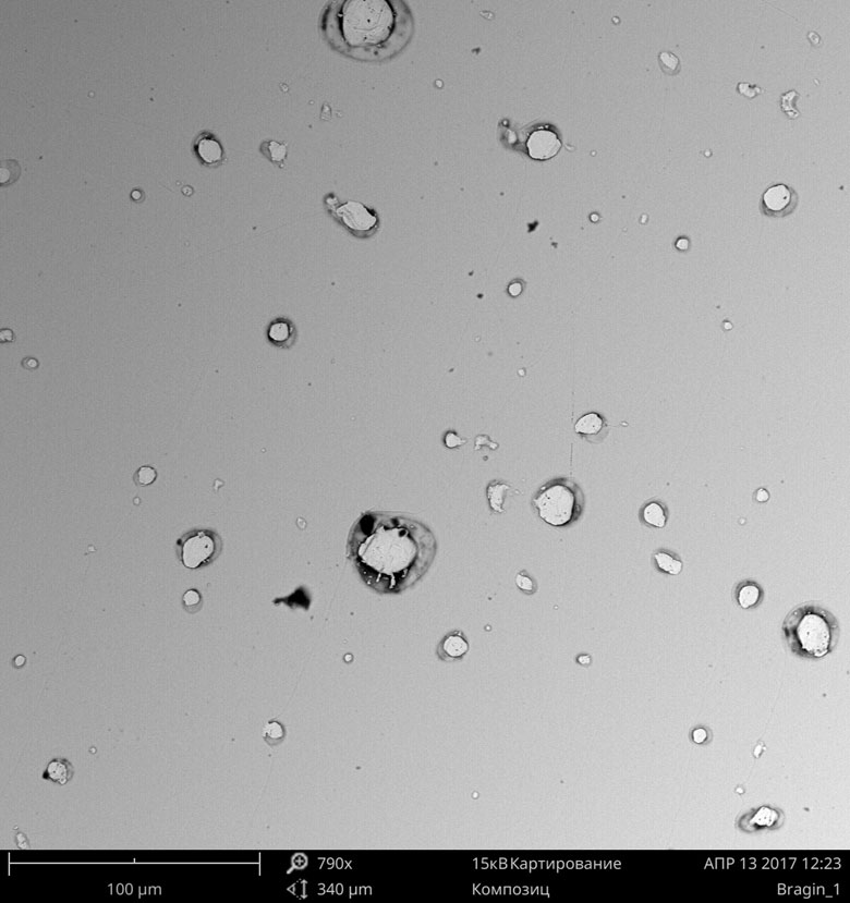
At present, with the development of semiconductor detectors of reflected electrons, it is not difficult to obtain such a contrast. For example, a photo from the past video about gallium antimonide:
Even with an accelerating voltage of 15kV, the compositional contrast is strongly noticeable.
1960
Thomas Everhart and Richard Thornley have developed an improved version of the electron detector, which is named after them: Everhart-Thornley Detector. This is the most common detector used in scanning electron microscopes to this day. In fact, the principle itself has remained unchanged since 1942. Novelty was added to the detection of elastically reflected electrons, where semiconductor sensors are widely used.
What did Everhart and Thornley offer? Schematically it looks like this:
Figure from [5].
In the vacuum chamber of the microscope, next to the sample is a Faraday cage 1. Inside it is a luminescent screen 3 ( scintillator ), which emits photons when electrons hit it. These photons through fiber 2 go beyond the vacuum chamber and enter the photomultiplier, where they are converted back into electrons at the photocathode and amplified many times due to the emission of secondary electrons on the dinodes inside the photomultiplier.
In order not to make an immersion lens, like Zvorykin, and not to keep an object table at 800 V potential, the Faraday 1 cell performs the function of a collector: a positive potential of about 200-400 V is applied to it, which attracts secondary electrons with low energies but little effect on the main electron beam.
But electrons with energies of the order of hundreds of eV will not lead to the excitation of the phosphor and the emission of a sufficient number of photons. Therefore, the scintillator 3 (if it is metallized, if not, you have to make an electrostatic lens around it), an accelerating voltage of about 12kV is applied, which is guaranteed to excite the phosphor. By the way, if there were no Faraday 1 cell, then this voltage would have a significant impact on the main beam, strongly rejecting it.
Metallized scintillator.
It would seem that a lot of unnecessary transformations, but "it just works."
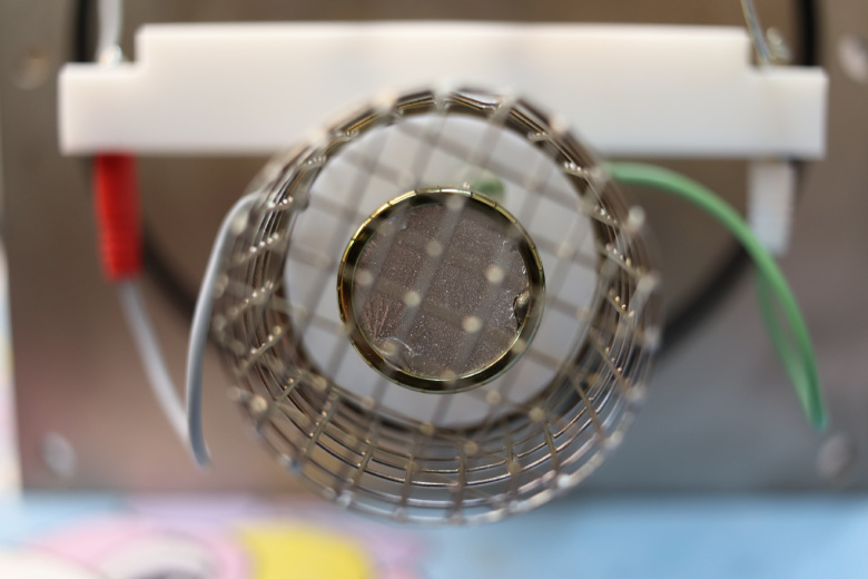
At the beginning of the article, I took a photograph of the vacuum part of the Everhart-Thornley detector, where one can visually see the Faraday cage, the metallized scintillator, the wires that supply accelerating voltage, and so on.
And this is how the photomultiplier tube sees
In the following series
Now you can make your own Everhart-Thornley detector for our JEOL, an absorbed current amplifier, and try to make a semiconductor detector of reflected electrons.
PS
One year has passed since the first publication. During this time, I managed to learn a lot, in many ways to figure it out, and share it with you. Meet with very interesting people who have greatly helped the project. And, write ten articles about the electron microscope in the garage.
Of course, I wanted to bring the project to the first image to this date, but was very busy. Nevertheless, on the way new articles about electronics, experiments with an electron beam and a lot more - I hope you like it! Immediately after the release of each article, I check the comments every few minutes, who writes what, whether they approve, whether there are any inaccuracies that need correction. Throughout the year, this feedback is the main motivation to continue working on the project.
Happy New Year!
Sources:
1. P.Hoks. Electron optics and electron microscopy. Moscow 1974.
2. THE SCANNING ELECTRON MICROSCOPE. A Small World of Huge Possibilities.
3. SCANNING ELECTRON MICROSCOPY 1928–1965. D. McMullan, Cavendish Laboratory, University of Cambridge, UK.
4. www.rfcafe.com/references/radio-craft/scanning-electron-microscope-september-1942-radio-craft.htm
5. Bykov Yu.A., Karpukhin S.D. Scanning electron microscopy and X-ray microanalysis. Tutorial. MGTU them. N.E. Bauman.
All Articles