Processor Design (CPU Design) Logisim
Part I
Part II
Part III
Part IV
Part V
One of the chapters of the book “Code” by Charles Petzold is devoted to designing a CPU and at the beginning of the chapter describes a device that allows you to summarize sets of numbers stored in memory. Let's design this scheme in Logisim. Let's take a set of eight-digit numbers and connect it to the multiplexer, transfer from one number to another will be done using a counter connected to the multiplexer select input, and connect the adder and the battery to the multiplexer output. We will use a button as a clock generator. Data will be loaded into the battery when the button is released (this is done using the NOT element connected to the button).
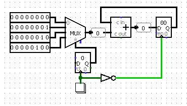
We will store the numbers in the RAM (RAM).
RAM can be represented as a set of registers accessed using a demultiplexer and multiplexer (DMX and MUX).
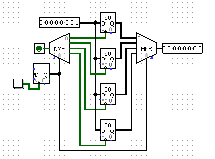
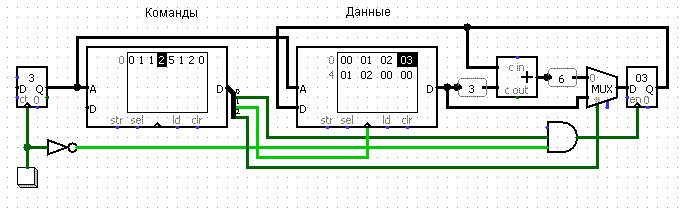
Suppose a set of numbers is stored in RAM, and we need to add all the numbers and save the result (in a free cell). We will store the commands (“add” and “save”) in one RAM, and the processed numbers - in the other. This method of storage is the hallmark of Harvard architecture .
The “1” command will write the number from the adder to the battery, the “2” command will write the number from the battery to the 2nd RAM.
Suppose several arrays of numbers are stored in RAM. Those. We need
We will use a MUX multiplexer for sampling data from RAM.
The new instruction "5" on the leading edge of the clock generator switches the MUX multiplexer, and on the falling edge (on a decay) writes to the battery.
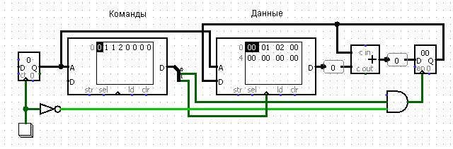
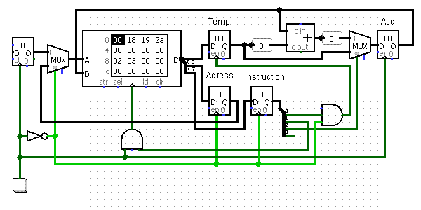
Next, we will store instructions and data in one RAM. This method of storage is the hallmark of the von Neumann architecture .
In the first four digits of the eight-bit memory cell, the command will be stored, in the second four digits, the address ( direct addressing ) will be stored.
We will load the address and command into separate registers, and then use the multiplexer to go to the saved address. To write data to the RAM, we will first load the data into the Temp temporary register (otherwise, instructions, not data, will be written into the RAM), and then into the accumulator Ass. Data recording in Temp and Ass will be performed on the falling edge.
We will add, for example, the numbers 2 and 3, which lie in cells 8 and 9, and store the result in the cell with the address a.
We also add the ability to make unconditional transitions.
We implement a device in which only one command will be executed - an unconditional branch command. To do this, we will send four low-order digits (the address itself) to the counter that generates the address, and we will send the command stored in the high-order digits of the memory cell to the download port.
For example, to jump into a cell with address 2, use the command 82.
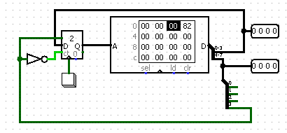
Add an unconditional jump to the previous scheme.
In general, there was already an article on geektimes devoted to designing a CPU in Logisim.
All schemes presented above can be downloaded in one file .
Logisim can be downloaded here .
Consider how the adder on the example of the chip 155im3 (7483). For the 155 series microcircuits, let's agree that there is an internal resistor at the inputs pulling to the positive (if the leg is “hanging in the air”, then there is a logical “unit” on it), so when the power supply is connected to the microcircuit, all the LEDs connected to the output .
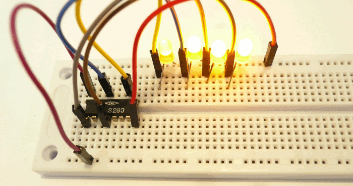
The picture shows MC 74ls283 (modern analogue 155im3).
In order to design such a microcircuit in Logisim, it is necessary to select “Menu” - “Project” - “Add schema”.
Here is how this MS looks inside a subcircuit. These are four half- adders, combined into a full adder.

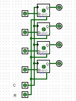
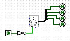
As the battery, we will use the 155TM8 (74175) microcircuit - quad D-flip-flop.
The triggers that are part of the MS pass through all the time while there is 1 at the synchronization input, not only along the front (triggers with static control), but in the Logisim program only triggers with dynamic control are available to us, but in this case it doesn’t matter ; we will use what is.
More about triggers can be found in Wikipedia.
We will assemble the MS 155tm8 model from D-flip-flops.
Further we will collect the scheme, allowing to put sets of numbers.
For example, if you add up a set of numbers 2 (0010), we get 2 (0010), 4 (0100), 6 (0110), etc.
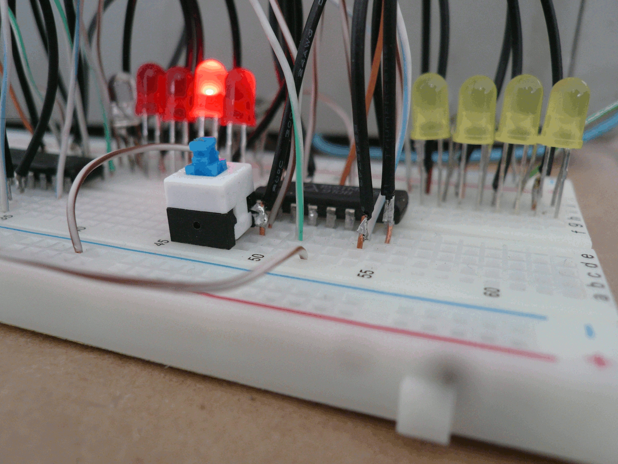
First, 2 appears at the output of the adder (red LEDs), then 2 is loaded into the quad D-Trigger (yellow LEDs), and 4 appears at the output of the adder, then 4 is loaded into 155m8, and 6 appears at the output of the adder.
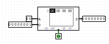
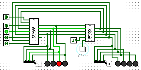
In order to design a simple memory module, we need a multiplexer. Let's design the dual multiplexer 155kp2.

We also need a counter. We will design the chip 155e5.
This is a four-digit counter, but we only need two lower digits.
Let us store numbers, for example, 2 (0010), 3 (0011), 5 (0101).
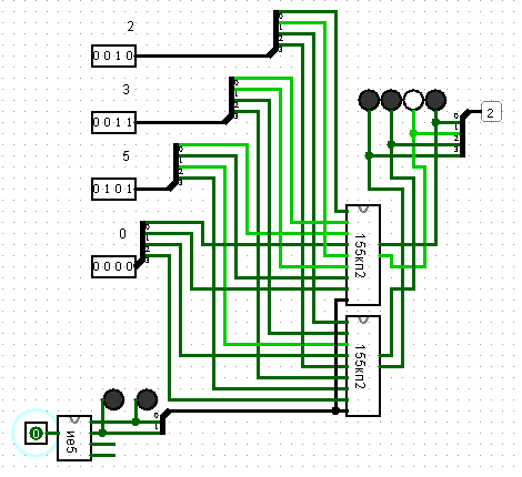
Let's unite all components in one scheme. We will add the numbers that are stored in the "memory"
2 + 3 + 5.
PS Article about the book “Code. The secret language of computer science. "Is on Habré here .
Part II
Part III
Part IV
Part V
One of the chapters of the book “Code” by Charles Petzold is devoted to designing a CPU and at the beginning of the chapter describes a device that allows you to summarize sets of numbers stored in memory. Let's design this scheme in Logisim. Let's take a set of eight-digit numbers and connect it to the multiplexer, transfer from one number to another will be done using a counter connected to the multiplexer select input, and connect the adder and the battery to the multiplexer output. We will use a button as a clock generator. Data will be loaded into the battery when the button is released (this is done using the NOT element connected to the button).
We will store the numbers in the RAM (RAM).
RAM can be represented as a set of registers accessed using a demultiplexer and multiplexer (DMX and MUX).
Suppose a set of numbers is stored in RAM, and we need to add all the numbers and save the result (in a free cell). We will store the commands (“add” and “save”) in one RAM, and the processed numbers - in the other. This method of storage is the hallmark of Harvard architecture .
The “1” command will write the number from the adder to the battery, the “2” command will write the number from the battery to the 2nd RAM.
Suppose several arrays of numbers are stored in RAM. Those. We need
- load numbers from ram to battery
- load numbers from adder to battery
- save numbers from battery to RAM
We will use a MUX multiplexer for sampling data from RAM.
The new instruction "5" on the leading edge of the clock generator switches the MUX multiplexer, and on the falling edge (on a decay) writes to the battery.
Next, we will store instructions and data in one RAM. This method of storage is the hallmark of the von Neumann architecture .
In the first four digits of the eight-bit memory cell, the command will be stored, in the second four digits, the address ( direct addressing ) will be stored.
We will load the address and command into separate registers, and then use the multiplexer to go to the saved address. To write data to the RAM, we will first load the data into the Temp temporary register (otherwise, instructions, not data, will be written into the RAM), and then into the accumulator Ass. Data recording in Temp and Ass will be performed on the falling edge.
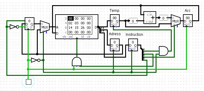
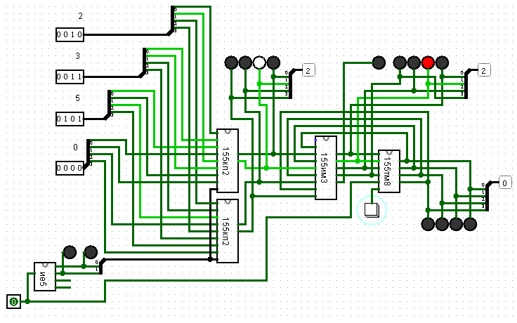
We will add, for example, the numbers 2 and 3, which lie in cells 8 and 9, and store the result in the cell with the address a.
We also add the ability to make unconditional transitions.
We implement a device in which only one command will be executed - an unconditional branch command. To do this, we will send four low-order digits (the address itself) to the counter that generates the address, and we will send the command stored in the high-order digits of the memory cell to the download port.
For example, to jump into a cell with address 2, use the command 82.
Add an unconditional jump to the previous scheme.
In general, there was already an article on geektimes devoted to designing a CPU in Logisim.
All schemes presented above can be downloaded in one file .
Logisim can be downloaded here .
Consider how the adder on the example of the chip 155im3 (7483). For the 155 series microcircuits, let's agree that there is an internal resistor at the inputs pulling to the positive (if the leg is “hanging in the air”, then there is a logical “unit” on it), so when the power supply is connected to the microcircuit, all the LEDs connected to the output .
The picture shows MC 74ls283 (modern analogue 155im3).
In order to design such a microcircuit in Logisim, it is necessary to select “Menu” - “Project” - “Add schema”.
Here is how this MS looks inside a subcircuit. These are four half- adders, combined into a full adder.
As the battery, we will use the 155TM8 (74175) microcircuit - quad D-flip-flop.
The triggers that are part of the MS pass through all the time while there is 1 at the synchronization input, not only along the front (triggers with static control), but in the Logisim program only triggers with dynamic control are available to us, but in this case it doesn’t matter ; we will use what is.
More about triggers can be found in Wikipedia.
We will assemble the MS 155tm8 model from D-flip-flops.
Further we will collect the scheme, allowing to put sets of numbers.
For example, if you add up a set of numbers 2 (0010), we get 2 (0010), 4 (0100), 6 (0110), etc.
First, 2 appears at the output of the adder (red LEDs), then 2 is loaded into the quad D-Trigger (yellow LEDs), and 4 appears at the output of the adder, then 4 is loaded into 155m8, and 6 appears at the output of the adder.
In order to design a simple memory module, we need a multiplexer. Let's design the dual multiplexer 155kp2.
We also need a counter. We will design the chip 155e5.
This is a four-digit counter, but we only need two lower digits.
Let us store numbers, for example, 2 (0010), 3 (0011), 5 (0101).
Let's unite all components in one scheme. We will add the numbers that are stored in the "memory"
2 + 3 + 5.
PS Article about the book “Code. The secret language of computer science. "Is on Habré here .
All Articles