DNA sequencing at home: how to assemble a device on the knee for 10 million
Hello everyone, my name is Alexander Sokolov, and I want to tell you how the sequencer, a DNA decryption device, did at home. The market price of such a device is about 10 million rubles.
A brief digression to genetics. If suddenly you remember, in 2003 a sensational statement was made: scientists finally deciphered the human genome. The genome is built from DNA, and DNA is the source code of the organism. DNA is a double strand consisting of 4 types of nucleotides that are repeated about 3 billion times in the human genome. Just as in bits all the information on your computer is encrypted, instructions about the assembly of all proteins of the human body are encoded in the nucleotides. That is, knowing the sequence in which the nucleotides are located in the DNA, we can theoretically gather all the necessary proteins and obtain a human model. So in the standard sense, scientists did not decipher the DNA, but simply transferred the chemical sequence to a set of zeros and ones on the computer. What to do next is a separate conversation. For example, at the moment, only 5% of the entire genome array is clear for us (this is protein coding). What do the remaining 95%, we can only guess.
In 2003, the cost of sequencing human DNA was about $ 100 million. Over time, this figure has decreased and now it is approaching a thousand dollars. You pay, your DNA is sequenced and they give you a hard disk with 3 GB of information - your genome in digital form.
There are three main sequencer on the market today. The most productive, Hiseq, and its receiver NovaSeq, provides the cheapest (fluorescent) sequencing. One of its launch lasts for several days, and during this time the genomes of several people are processed at once. However, the launch itself costs about ten thousand dollars. By the way, the device itself costs about $ 1 million, and since it becomes obsolete in about 3 years, in order for it to pay off, it must bring you $ 1,000 a day.
The second device appeared on the market last summer. It is called Nanopore and is based on a very interesting technology, when DNA is sequenced by passing through a nanopore. The cheapest version of Nanopore is positioned as a disposable home sequencer and costs $ 1000.
The third device is a PGM, a semiconductor sequencer, which costs $ 50,000 at home and about 10 million rubles (with delivery, customs clearance, etc.) in Russia. The process of sequencing on it takes about several hours.
Well, I didn't have ten millions, but PGM wanted to. I had to do it myself. First, briefly how semiconductor sequencing occurs. The entire DNA strand is divided into fragments of 300-400 nucleotides in length, called reads. Then the reads attach to small spheres and are copied many times - as a result, a whole bunch of identical DNA fragments “hang” on each sphere. Copying is necessary to enhance the signal from each particular read. A set of different spheres is called a DNA library.
The heart of the PGM is a disposable chip - a matrix similar to the matrix in the camera, only instead of pixels that react to light, here the pH transistors react to changes in the acid-base balance. The resulting library of DNA is loaded onto a chip containing 10 million wells, at the bottom of each of them is a pH transistor. Only one sphere can fit in a well and, therefore, reads of only one type (with one specific nucleotide sequence). Next, reagents are fed to the chip in such a way that the DNA starts copying itself. And it is copied linearly, that is, the nucleotides are attached to the newly created chain in the order in which they stand in the parent chain. Therefore, one type of nucleotide is fed to the chip - and a change in pH is immediately detected in some wells (this means that the nucleotide has been attached to them). Then another type of nucleotide is supplied and the pH change in the wells is recorded, etc. Thus, by submitting all 4 types of nucleotides to the chip many times, we can get information about the sequence of nucleotides in each read. Then, in mathematical ways, read short segments are collected on a computer in a single chain. To collect it more or less confidently, each read must be read about 100 times.
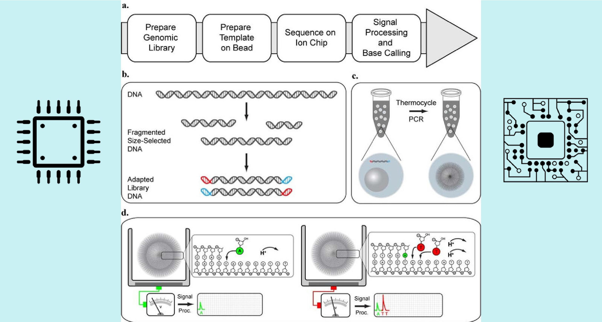
Fig.1. Semiconductor sequencing
Now let's figure out what the device consists of. There is, as we already know, a chip, as well as a reagent supply system and a motherboard. All sequencing is done on the chip — the rest of the device only transmits certain signals to it, delivers reagents, reads analog signals from it, digitizes them, and drives the resulting information stream to a computer, where data is accumulated and processed.
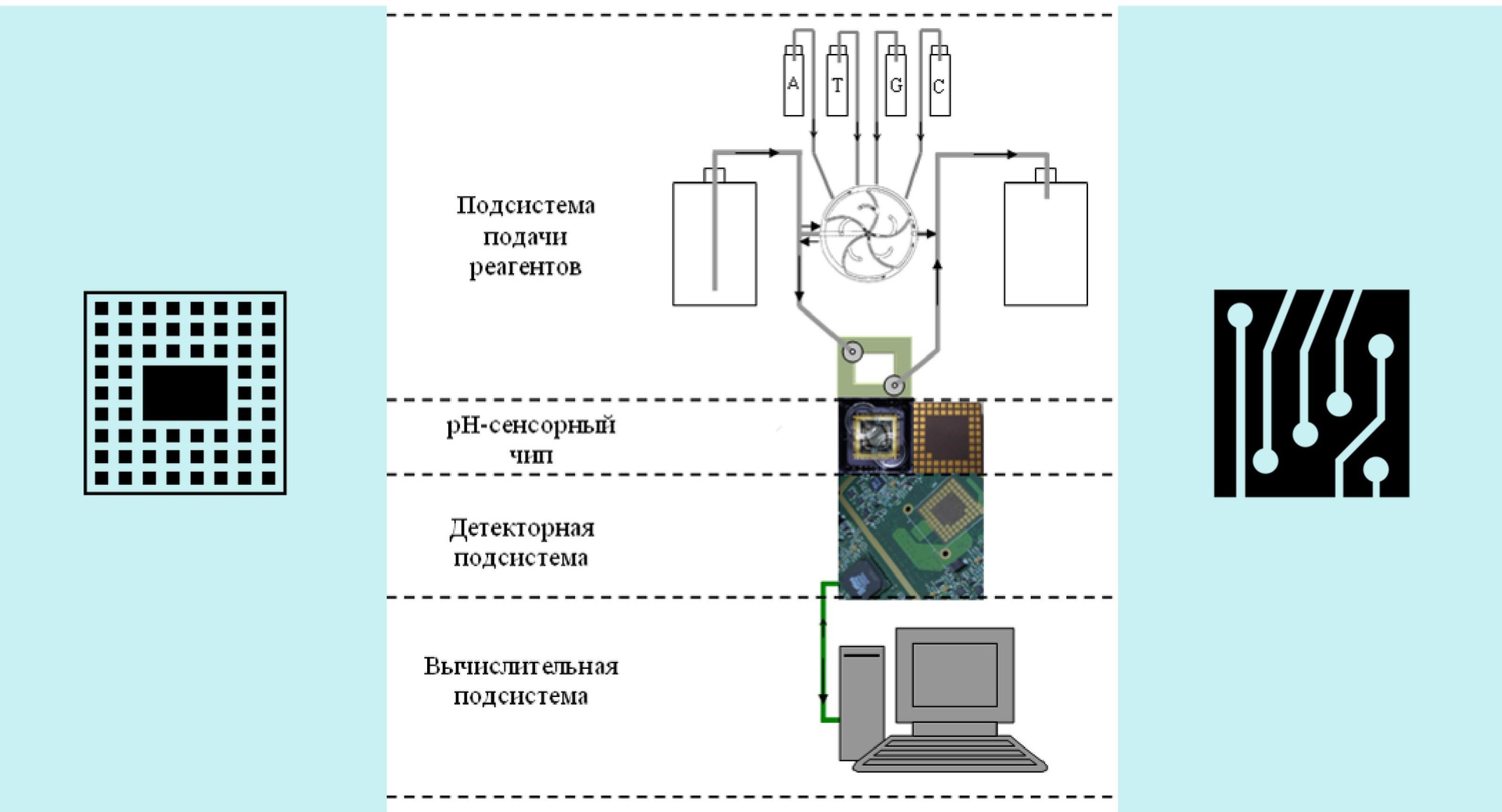
Fig. 2. Device sequencer
The chip is positioned as a disposable and is discarded after use. Accordingly, where PGM works, such chips can be obtained free of charge in any quantity. Why get them, you ask? The fact is that I have already managed to use the chip many times. In fact, it is eternal: it is enough to rinse it well enough - and you can apply it again and again. In terms of accuracy, it will not differ from the new. My very idea was to make a device for this conditionally free chip.
So, I faced the challenge of reverse engineering of the chip. Of course, it was impossible to find any documentation for the cherished microcircuit - the manufacturer was not going to share production secrets, but wanted to quietly sell their devices for $ 50,000. To begin with, I did the most obvious and simple: I rang the contacts with a tester. It became clear where the digital and analog inputs-outputs, power, and so on. Some information was learned from the patents on the chip. But all this, of course, was not enough to create a complete product. I still fiddled with the chip, checked my various guesses, experimented with signals, but didn’t go anywhere in principle. I had to pause the project.
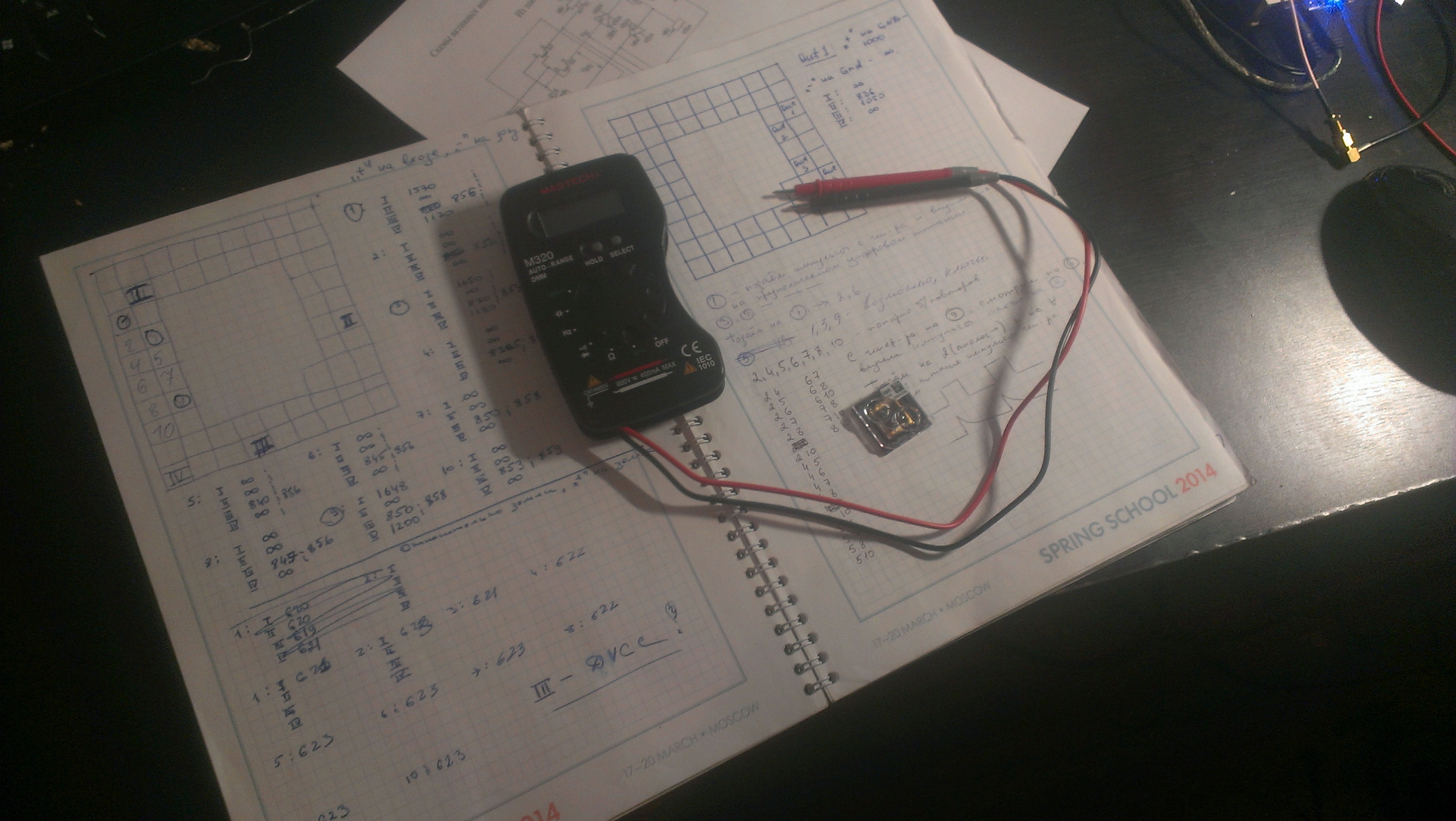
Fig. 3. Ping chip
And then suddenly on Habrahabr I came across an article by the famous blogger BarsMonster about how he does reverse-engineering of chips! He was inspired, wrote to him, wrote to other enthusiasts, sent a request to Kiev, where they were engaged in photographing chips. From Kiev they answered that they could not polish in layers, they could only capture the top layer, and since my chip is multi-layered, it will not be clear where the tracks from the contacts go. Then he met one American, who also engaged in reverse engineering of chips, sent him his chips, but even then it didn’t go further photographing the upper layer. Then I came across an article on the Internet about those who were able to reverse the Sony PlayStation chip, etc. (“Glory to the heroes!” And that’s all, if anyone knows). I decided to write them with questions, found their nicknames - and immediately realized that one of them was familiar to me. Recently, a friend brought me to a friend who “is also engaged in genetics at the amateur level,” we talked to this friend on Skype and ended the dialogue. And now I understand that my new friend is a mega-cool master reverse-engineering chips. Immediately wrote to him. However, it turned out that, although he was ready to help, he did not have a microscope. Again a dead end.
A few months later, the required microscope was found in a nearby laboratory! True, the camera built into it was terrible, I photographed on my mobile phone through the eyepiece and got pictures of this quality:

Fig. 4. Chip under the microscope
Then, on the last New Year, an excellent microscope for 130 thousand appeared at my work (I am a specialist in quantum cryptography). Dreams Come True. Finally, I was able to properly photograph the chip on top.
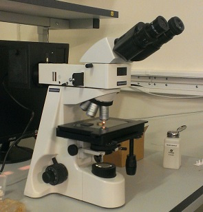
Fig. 5. My working microscope
And then ... Then I still had to master the technique of polishing it myself. The difficulty of polishing is to remove the layers of metal with a thickness of about 1 micron - and the width of the chip is 1 centimeter. For comparison, I will say that this is about the same as allowing an error of not more than 10 cm per 1 km. I tried very hard. The results of my work are presented in the following photo:
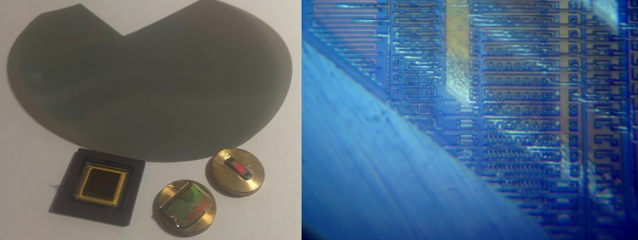
Fig. 6. Reverse engineering under an optical microscope.
The lower silicon layer, the top layer with transistors, the first, second, third, and fourth layers of metal are quite clearly visible.
The chip consists of repeating zones (such as shift registers), and from such pictures it was very convenient to analyze it: it immediately became clear what was happening on different layers. I "reversed" the most "stuffed" areas with an abundance of logic that were repeated many times. But it turned out to be the most difficult to track the tracks going across the chip, to understand which external contact belongs to what. From the New Year's holidays to the end of February, I, armed with a new beautiful microscope, pored over this task - I sat at work until ten at night, “reversil,” thought. And then a new miracle happened: a friend was able to organize free photography of the chip in layers on an electron microscope at MIREA. "Photosession" crumbs in 1 square. cm represented a 50 GB of black and white photographs.
Now all these separate photos needed to be somehow united into one whole picture. Almost the same day I wrote a program on the Python that generated the HTML file - when I opened it in the browser, I got what I needed. (By the way, the oldest 10th Opera coped with this best of all, I recommend!) Then I wrote another program in javascript that allows me to compare layers, smoothly move between them, align them, adjust the scale, etc. Finally, in my hands There were all the tools to solve the main tasks. I traced the chip penetrating tracks and restored its entire structure to the last transistor.
Another photo of the chip section taken under X-ray (at MIREA):
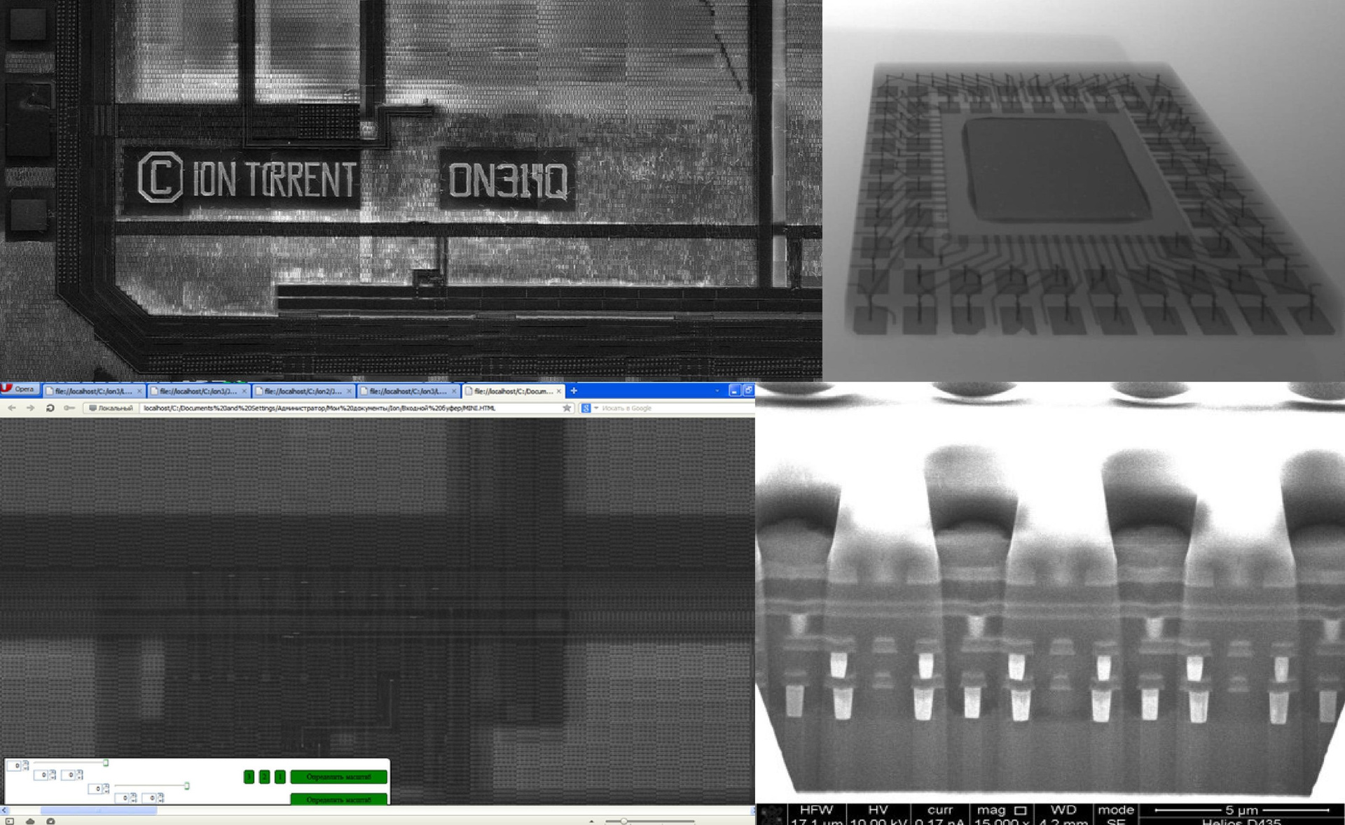
Fig. 7. Shooting under the electron microscope
The holes are clearly visible where the spheres with the reads fall. Below are three layers of metal, and even lower - a layer with transistors.
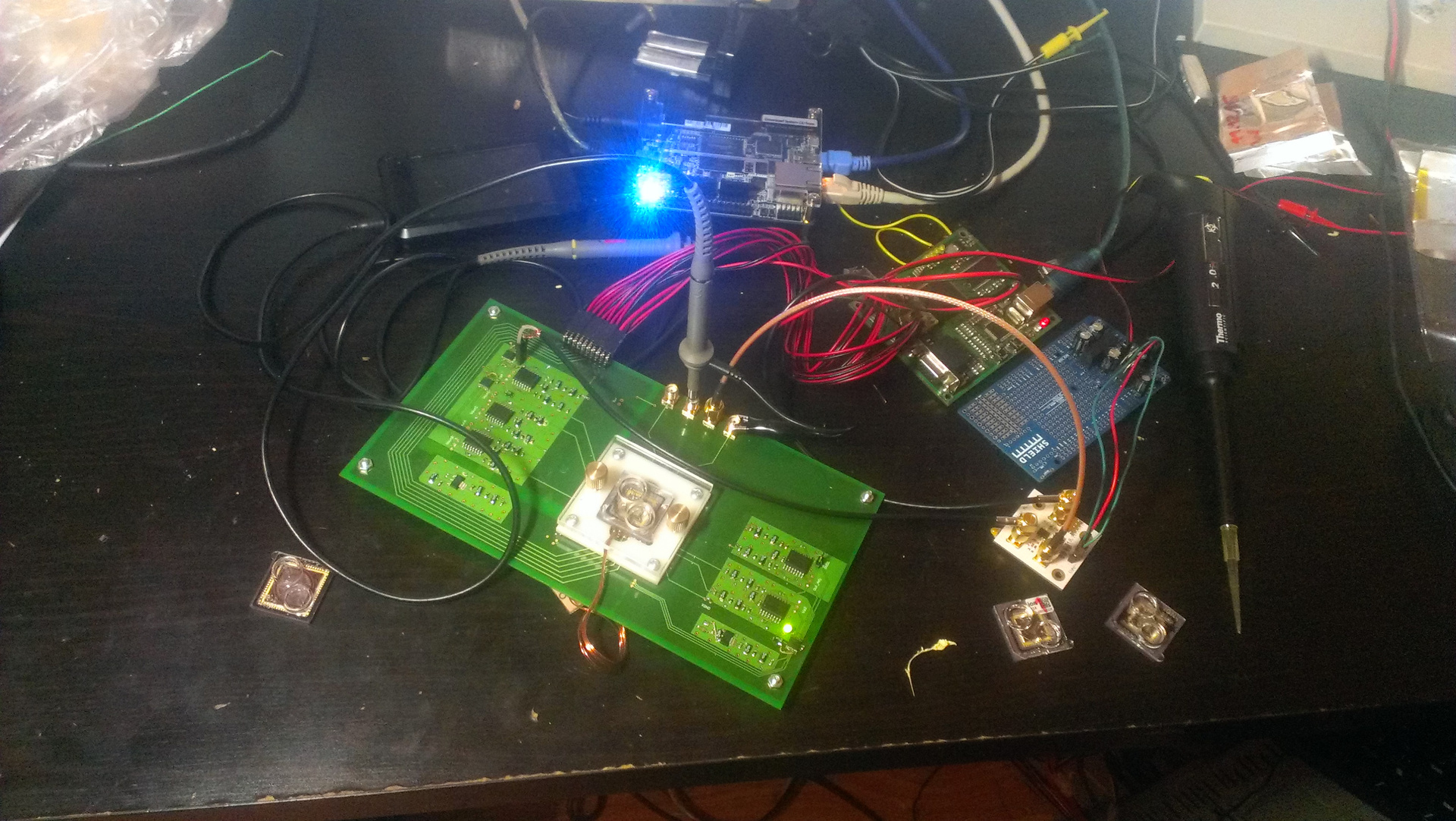
The next stage of the struggle for a brighter future was the creation of a motherboard for the chip. Designed it and sent an order for production. In the meantime, the court used the Mars Rover-2 board with FPGA to work with the chip. (FPGA is, roughly speaking, an array of 10,000 universal logic elements; by programming FPGA, we can get any logic that easily processes gigabit data streams.) I wrote the firmware for FPGA myself, and besides, I wrote software for dynamic control of the system which sets the entire configuration for FPGA. Then a semi-annual break formed again (he went on a business trip to Baikal, he prepared a setup in the laboratory, which was demonstrated to Putin). But in the end the stars came together: I had time, ready-made boards arrived - and I collected my system.
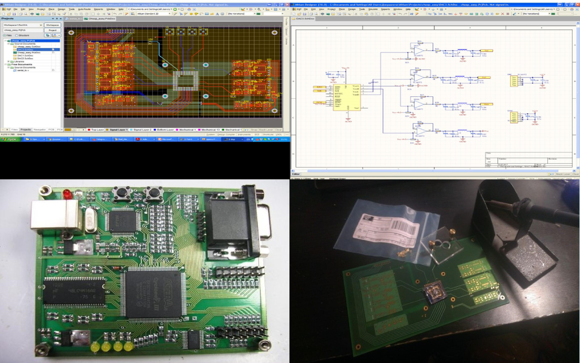
Fig. 8. Creation of "iron"
Gave all the necessary signals and - oh, a miracle! - I saw a signal from the chip on the oscilloscope. (I bought an oscilloscope sometime for 6,000 rubles on eBay, another 1,000 cost the firmware to it.) The spots are clearly visible on the picture - droplets of some kind of reagent.
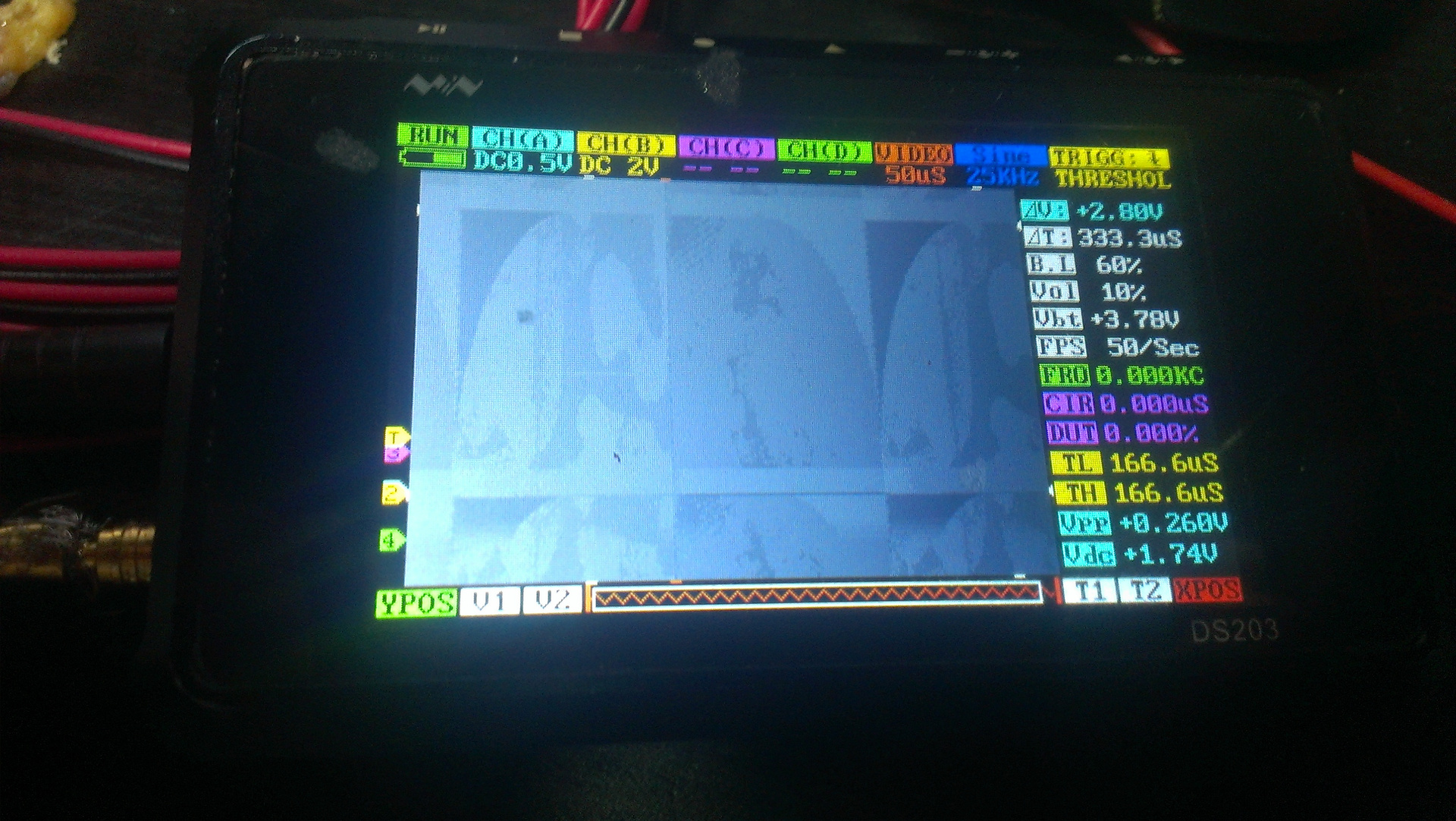
Fig. 9. Signal from the chip on the oscilloscope
Now I had to figure out how to digitize this picture and transfer it to a computer. I put together such an installation:
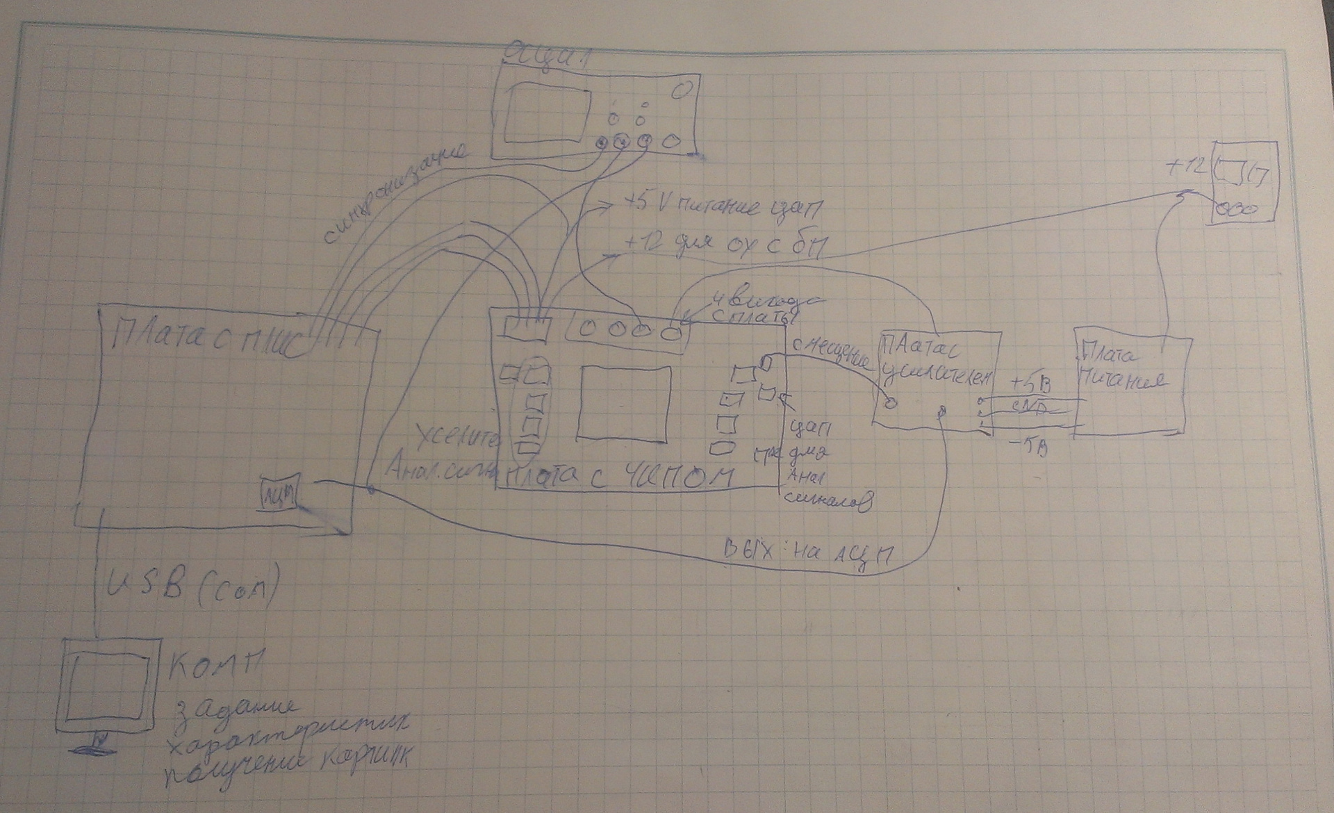
Fig.10. Device layout
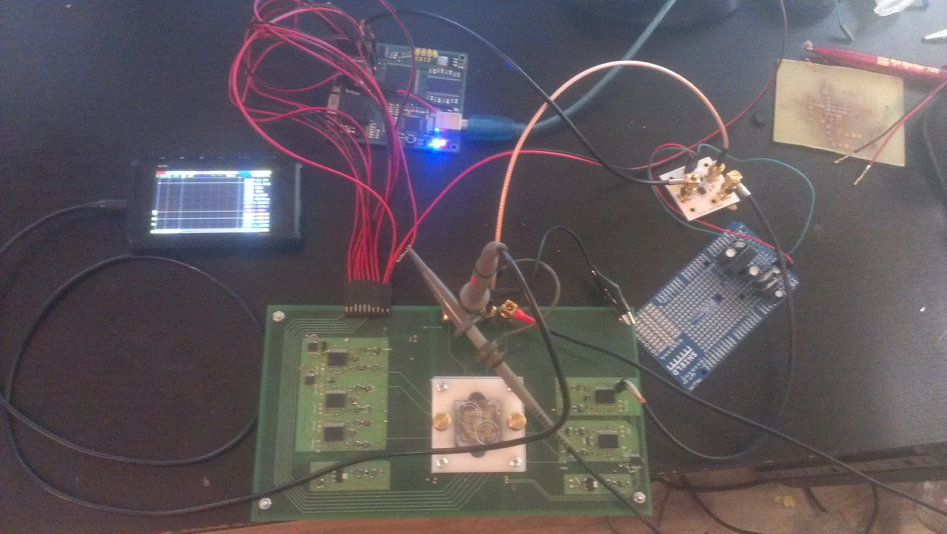
Fig. 11. Ready installation
There is a computer that supplies control data to the board with FPGA. The board generates digital signals and sends them to the chip. The signal from the chip goes to the amplifier, then - to the ADC on the board, digitized and transmitted via the COM port to the computer. In general, the bandwidth of the COM port is small: 15 kilobits per second (because there is from 1 million to 10 million "pixels" in one chip, and the maximum transfer rate is 115200 baud). Nevertheless, the picture on the computer eventually falls.
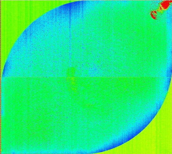
Fig. 12. The processed signal on the computer.
The photo above shows that when the DNA library is fed to the used b / w chip, the chip is filled unevenly: at the edges - to a lesser extent. Different colors due to different voltages on the pH transistors. That is, we can clearly distinguish those wells into which the spheres with reads are located — subsequently this will help us control the flushing of the chip.
Accordingly, the next task was flushing the chip. It was necessary to ensure that he became like new. Fortunately, I had a completely new chip as a reference sample. On ill. And it is clear that in the active area such a chip is almost of the same color (vertical repeating stripes are just noises, pickups).
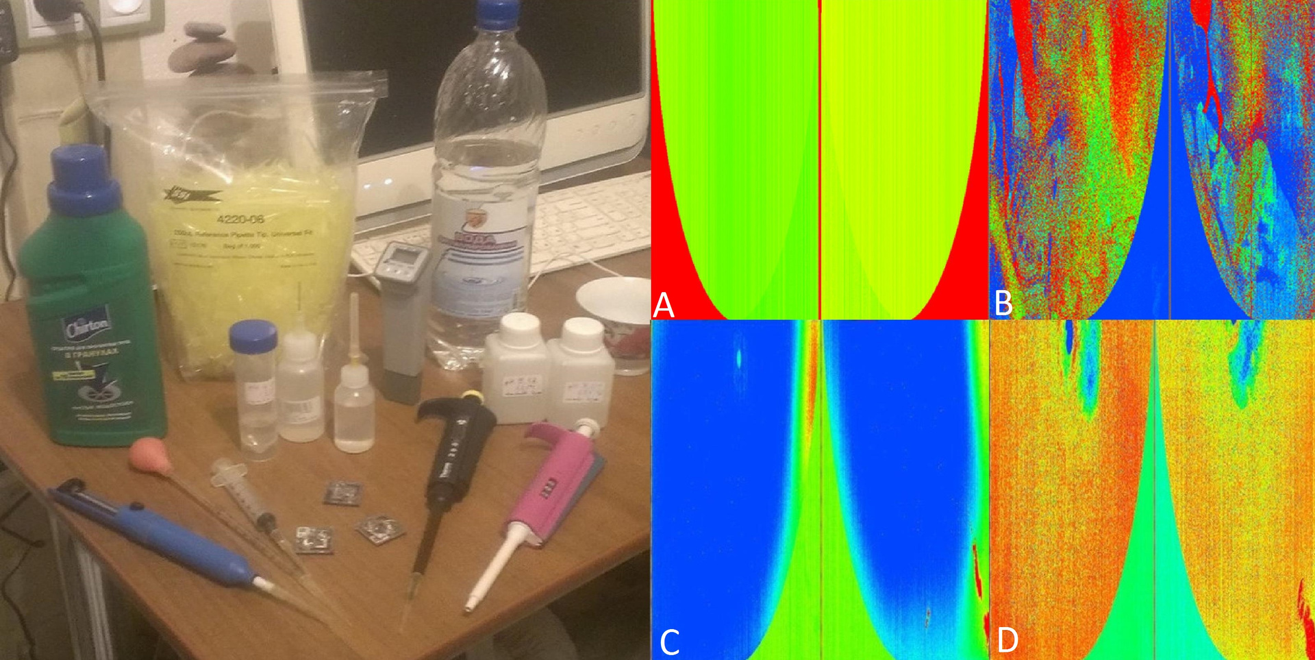
Fig. 13. Flushing the chip
In fig. 13 B unsuccessfully washed chip - it is multi-colored. In Figure 13, D is a used but well washed chip. It is seen that the gradient at the edges has disappeared. Nevertheless, it would be worthwhile to prove that it is really clean and can be reused.
Since the DNA libraries are attached to the tantalum coating of the chip in an acidic medium and are detached in an alkaline (i.e., at high pH), the chip is washed with special semi-automatic pipettes with solutions with different pH. Today I managed to achieve almost complete chip cleaning.
I was interested in why, when I fully understood the structure of the chip, I did not order to make it, but preferred to continue to search and retrieve the used ones, to mess with their washing, and so on. Yes, because the development of the chip costs a lot of money, millions of dollars, and a substantial part of this amount goes to the physical debugging of the resulting product: fitting, setting all the parameters of transistors, etc. That is, just copying the logic circuit is not enough. Therefore, I take a conditionally free, ready-made - designed, manufactured, debugged - microcircuit and thus save significant funds, seriously reduce the cost of the project.
My next task was to collect a more advanced device that would allow transferring information to a computer faster and at the same time would not consist of a huge number of individual boards.
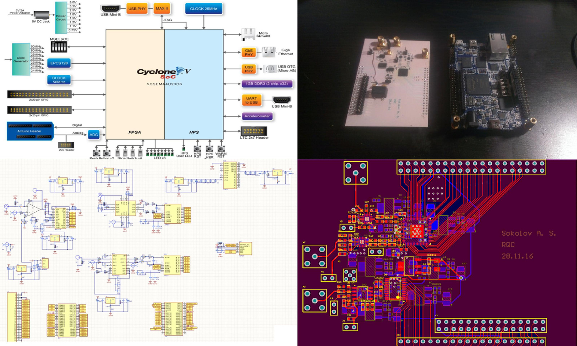
Fig.14 Development of the next version of the device
I took a new board with FPGA - on the same chip there were 2 ARM-cores with Linux, there was a Gigabit Ethernet and other “buns”, but, unlike the previous version, there was no ADC. Later I designed another motherboard, with high-speed ADCs and all the other necessary elements. Launched - it all worked.
What is left to do for the appearance of the final device? Only three things.
The first. Need gigabit internet, fast data transfer to a computer. I realized this just yesterday.
The second. Reagent supply system. Designing a special valve is already in process.
Third. Software for processing information from the chip. I still have questions with software, so I invite programmers to cooperate.
The final device is worth 10 million rubles. The cost of sequencing is several thousand dollars. Chips cost from 100 to 1000 dollars - depending on the number of "pixels" in them. (By the way, the recovery of chips in itself can be a good earning, especially considering that only a couple of clicks need to be done for flushing.) Reagents are also bought, but in the future they will also be created.
In general, all this is very interesting, but the main thing is the future. Today biotechnologies occupy the same place in the world scientific and technical progress as computer technologies in the 80s. last century. At the same time, sequencing is one of the key areas for modern biology and medicine. And, of course, biotechnology is very profitable.
Recently, the semiconductor sequencer S5 has appeared on the market, and in the near future I plan to switch to it.
I will be glad to talk with anyone who wants to participate in the development of this project in one way or another!
The project would not have been possible, without the theoretical training of Vladimir Zubov . I express my gratitude to him.
Thanks for attention!
A brief digression to genetics. If suddenly you remember, in 2003 a sensational statement was made: scientists finally deciphered the human genome. The genome is built from DNA, and DNA is the source code of the organism. DNA is a double strand consisting of 4 types of nucleotides that are repeated about 3 billion times in the human genome. Just as in bits all the information on your computer is encrypted, instructions about the assembly of all proteins of the human body are encoded in the nucleotides. That is, knowing the sequence in which the nucleotides are located in the DNA, we can theoretically gather all the necessary proteins and obtain a human model. So in the standard sense, scientists did not decipher the DNA, but simply transferred the chemical sequence to a set of zeros and ones on the computer. What to do next is a separate conversation. For example, at the moment, only 5% of the entire genome array is clear for us (this is protein coding). What do the remaining 95%, we can only guess.
In 2003, the cost of sequencing human DNA was about $ 100 million. Over time, this figure has decreased and now it is approaching a thousand dollars. You pay, your DNA is sequenced and they give you a hard disk with 3 GB of information - your genome in digital form.
There are three main sequencer on the market today. The most productive, Hiseq, and its receiver NovaSeq, provides the cheapest (fluorescent) sequencing. One of its launch lasts for several days, and during this time the genomes of several people are processed at once. However, the launch itself costs about ten thousand dollars. By the way, the device itself costs about $ 1 million, and since it becomes obsolete in about 3 years, in order for it to pay off, it must bring you $ 1,000 a day.
The second device appeared on the market last summer. It is called Nanopore and is based on a very interesting technology, when DNA is sequenced by passing through a nanopore. The cheapest version of Nanopore is positioned as a disposable home sequencer and costs $ 1000.
The third device is a PGM, a semiconductor sequencer, which costs $ 50,000 at home and about 10 million rubles (with delivery, customs clearance, etc.) in Russia. The process of sequencing on it takes about several hours.
Well, I didn't have ten millions, but PGM wanted to. I had to do it myself. First, briefly how semiconductor sequencing occurs. The entire DNA strand is divided into fragments of 300-400 nucleotides in length, called reads. Then the reads attach to small spheres and are copied many times - as a result, a whole bunch of identical DNA fragments “hang” on each sphere. Copying is necessary to enhance the signal from each particular read. A set of different spheres is called a DNA library.
The heart of the PGM is a disposable chip - a matrix similar to the matrix in the camera, only instead of pixels that react to light, here the pH transistors react to changes in the acid-base balance. The resulting library of DNA is loaded onto a chip containing 10 million wells, at the bottom of each of them is a pH transistor. Only one sphere can fit in a well and, therefore, reads of only one type (with one specific nucleotide sequence). Next, reagents are fed to the chip in such a way that the DNA starts copying itself. And it is copied linearly, that is, the nucleotides are attached to the newly created chain in the order in which they stand in the parent chain. Therefore, one type of nucleotide is fed to the chip - and a change in pH is immediately detected in some wells (this means that the nucleotide has been attached to them). Then another type of nucleotide is supplied and the pH change in the wells is recorded, etc. Thus, by submitting all 4 types of nucleotides to the chip many times, we can get information about the sequence of nucleotides in each read. Then, in mathematical ways, read short segments are collected on a computer in a single chain. To collect it more or less confidently, each read must be read about 100 times.
Fig.1. Semiconductor sequencing
Now let's figure out what the device consists of. There is, as we already know, a chip, as well as a reagent supply system and a motherboard. All sequencing is done on the chip — the rest of the device only transmits certain signals to it, delivers reagents, reads analog signals from it, digitizes them, and drives the resulting information stream to a computer, where data is accumulated and processed.
Fig. 2. Device sequencer
The chip is positioned as a disposable and is discarded after use. Accordingly, where PGM works, such chips can be obtained free of charge in any quantity. Why get them, you ask? The fact is that I have already managed to use the chip many times. In fact, it is eternal: it is enough to rinse it well enough - and you can apply it again and again. In terms of accuracy, it will not differ from the new. My very idea was to make a device for this conditionally free chip.
So, I faced the challenge of reverse engineering of the chip. Of course, it was impossible to find any documentation for the cherished microcircuit - the manufacturer was not going to share production secrets, but wanted to quietly sell their devices for $ 50,000. To begin with, I did the most obvious and simple: I rang the contacts with a tester. It became clear where the digital and analog inputs-outputs, power, and so on. Some information was learned from the patents on the chip. But all this, of course, was not enough to create a complete product. I still fiddled with the chip, checked my various guesses, experimented with signals, but didn’t go anywhere in principle. I had to pause the project.
Fig. 3. Ping chip
And then suddenly on Habrahabr I came across an article by the famous blogger BarsMonster about how he does reverse-engineering of chips! He was inspired, wrote to him, wrote to other enthusiasts, sent a request to Kiev, where they were engaged in photographing chips. From Kiev they answered that they could not polish in layers, they could only capture the top layer, and since my chip is multi-layered, it will not be clear where the tracks from the contacts go. Then he met one American, who also engaged in reverse engineering of chips, sent him his chips, but even then it didn’t go further photographing the upper layer. Then I came across an article on the Internet about those who were able to reverse the Sony PlayStation chip, etc. (“Glory to the heroes!” And that’s all, if anyone knows). I decided to write them with questions, found their nicknames - and immediately realized that one of them was familiar to me. Recently, a friend brought me to a friend who “is also engaged in genetics at the amateur level,” we talked to this friend on Skype and ended the dialogue. And now I understand that my new friend is a mega-cool master reverse-engineering chips. Immediately wrote to him. However, it turned out that, although he was ready to help, he did not have a microscope. Again a dead end.
A few months later, the required microscope was found in a nearby laboratory! True, the camera built into it was terrible, I photographed on my mobile phone through the eyepiece and got pictures of this quality:
Fig. 4. Chip under the microscope
Then, on the last New Year, an excellent microscope for 130 thousand appeared at my work (I am a specialist in quantum cryptography). Dreams Come True. Finally, I was able to properly photograph the chip on top.
Fig. 5. My working microscope
And then ... Then I still had to master the technique of polishing it myself. The difficulty of polishing is to remove the layers of metal with a thickness of about 1 micron - and the width of the chip is 1 centimeter. For comparison, I will say that this is about the same as allowing an error of not more than 10 cm per 1 km. I tried very hard. The results of my work are presented in the following photo:
Fig. 6. Reverse engineering under an optical microscope.
The lower silicon layer, the top layer with transistors, the first, second, third, and fourth layers of metal are quite clearly visible.
The chip consists of repeating zones (such as shift registers), and from such pictures it was very convenient to analyze it: it immediately became clear what was happening on different layers. I "reversed" the most "stuffed" areas with an abundance of logic that were repeated many times. But it turned out to be the most difficult to track the tracks going across the chip, to understand which external contact belongs to what. From the New Year's holidays to the end of February, I, armed with a new beautiful microscope, pored over this task - I sat at work until ten at night, “reversil,” thought. And then a new miracle happened: a friend was able to organize free photography of the chip in layers on an electron microscope at MIREA. "Photosession" crumbs in 1 square. cm represented a 50 GB of black and white photographs.
Now all these separate photos needed to be somehow united into one whole picture. Almost the same day I wrote a program on the Python that generated the HTML file - when I opened it in the browser, I got what I needed. (By the way, the oldest 10th Opera coped with this best of all, I recommend!) Then I wrote another program in javascript that allows me to compare layers, smoothly move between them, align them, adjust the scale, etc. Finally, in my hands There were all the tools to solve the main tasks. I traced the chip penetrating tracks and restored its entire structure to the last transistor.
Another photo of the chip section taken under X-ray (at MIREA):
Fig. 7. Shooting under the electron microscope
The holes are clearly visible where the spheres with the reads fall. Below are three layers of metal, and even lower - a layer with transistors.
The next stage of the struggle for a brighter future was the creation of a motherboard for the chip. Designed it and sent an order for production. In the meantime, the court used the Mars Rover-2 board with FPGA to work with the chip. (FPGA is, roughly speaking, an array of 10,000 universal logic elements; by programming FPGA, we can get any logic that easily processes gigabit data streams.) I wrote the firmware for FPGA myself, and besides, I wrote software for dynamic control of the system which sets the entire configuration for FPGA. Then a semi-annual break formed again (he went on a business trip to Baikal, he prepared a setup in the laboratory, which was demonstrated to Putin). But in the end the stars came together: I had time, ready-made boards arrived - and I collected my system.
Fig. 8. Creation of "iron"
Gave all the necessary signals and - oh, a miracle! - I saw a signal from the chip on the oscilloscope. (I bought an oscilloscope sometime for 6,000 rubles on eBay, another 1,000 cost the firmware to it.) The spots are clearly visible on the picture - droplets of some kind of reagent.
Fig. 9. Signal from the chip on the oscilloscope
Now I had to figure out how to digitize this picture and transfer it to a computer. I put together such an installation:
Fig.10. Device layout
Fig. 11. Ready installation
There is a computer that supplies control data to the board with FPGA. The board generates digital signals and sends them to the chip. The signal from the chip goes to the amplifier, then - to the ADC on the board, digitized and transmitted via the COM port to the computer. In general, the bandwidth of the COM port is small: 15 kilobits per second (because there is from 1 million to 10 million "pixels" in one chip, and the maximum transfer rate is 115200 baud). Nevertheless, the picture on the computer eventually falls.
Fig. 12. The processed signal on the computer.
The photo above shows that when the DNA library is fed to the used b / w chip, the chip is filled unevenly: at the edges - to a lesser extent. Different colors due to different voltages on the pH transistors. That is, we can clearly distinguish those wells into which the spheres with reads are located — subsequently this will help us control the flushing of the chip.
Accordingly, the next task was flushing the chip. It was necessary to ensure that he became like new. Fortunately, I had a completely new chip as a reference sample. On ill. And it is clear that in the active area such a chip is almost of the same color (vertical repeating stripes are just noises, pickups).
Fig. 13. Flushing the chip
In fig. 13 B unsuccessfully washed chip - it is multi-colored. In Figure 13, D is a used but well washed chip. It is seen that the gradient at the edges has disappeared. Nevertheless, it would be worthwhile to prove that it is really clean and can be reused.
Since the DNA libraries are attached to the tantalum coating of the chip in an acidic medium and are detached in an alkaline (i.e., at high pH), the chip is washed with special semi-automatic pipettes with solutions with different pH. Today I managed to achieve almost complete chip cleaning.
I was interested in why, when I fully understood the structure of the chip, I did not order to make it, but preferred to continue to search and retrieve the used ones, to mess with their washing, and so on. Yes, because the development of the chip costs a lot of money, millions of dollars, and a substantial part of this amount goes to the physical debugging of the resulting product: fitting, setting all the parameters of transistors, etc. That is, just copying the logic circuit is not enough. Therefore, I take a conditionally free, ready-made - designed, manufactured, debugged - microcircuit and thus save significant funds, seriously reduce the cost of the project.
My next task was to collect a more advanced device that would allow transferring information to a computer faster and at the same time would not consist of a huge number of individual boards.
Fig.14 Development of the next version of the device
I took a new board with FPGA - on the same chip there were 2 ARM-cores with Linux, there was a Gigabit Ethernet and other “buns”, but, unlike the previous version, there was no ADC. Later I designed another motherboard, with high-speed ADCs and all the other necessary elements. Launched - it all worked.
What is left to do for the appearance of the final device? Only three things.
The first. Need gigabit internet, fast data transfer to a computer. I realized this just yesterday.
The second. Reagent supply system. Designing a special valve is already in process.
Third. Software for processing information from the chip. I still have questions with software, so I invite programmers to cooperate.
The final device is worth 10 million rubles. The cost of sequencing is several thousand dollars. Chips cost from 100 to 1000 dollars - depending on the number of "pixels" in them. (By the way, the recovery of chips in itself can be a good earning, especially considering that only a couple of clicks need to be done for flushing.) Reagents are also bought, but in the future they will also be created.
In general, all this is very interesting, but the main thing is the future. Today biotechnologies occupy the same place in the world scientific and technical progress as computer technologies in the 80s. last century. At the same time, sequencing is one of the key areas for modern biology and medicine. And, of course, biotechnology is very profitable.
Recently, the semiconductor sequencer S5 has appeared on the market, and in the near future I plan to switch to it.
I will be glad to talk with anyone who wants to participate in the development of this project in one way or another!
The project would not have been possible, without the theoretical training of Vladimir Zubov . I express my gratitude to him.
Thanks for attention!
All Articles