Intel 8008 processor - what's inside?
It's hard to believe, but the Intel 8008 processor, the first of its kind, the forerunner of the gigantic x86 family of processors, came to light exactly 45 years ago - on April 1, 1972. The story of his birth, as you know , was quite confusing and, for sure, at that time very few people saw in him a future legend. Well, now I think that very few people will argue about the steepness and grandeur of the 8008 - it was really a milestone in chip design. Let's take a look inside this chip with the help of Ken Shirriff, an enthusiastic oldfaga and his microscope , and see how it works.
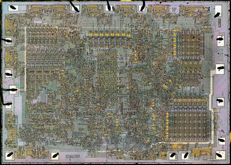
In front of you is the 8008 processor crystal in all its glory. The squares on the sides are platforms to which massive legs were soldered. On the chip, you see the inscriptions "8008" on the right and "Intel 1971" below. The HF initials from the top right belong to Hall Feeney (Hal Feeney) , who created the logical and physical scheme of the processor. Together with Feeney, Ted Hoff, Sten Mazor and Federico Faggin worked on the creation of the 8008.
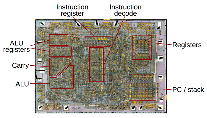
We now consider the constituent functional parts of our chip. On the left, we see an arithmetic logic unit (Arithmetic / Logic Unit, ALU) performing calculations on the available data. The ALU has two temporary registers for storing input data. As we see, they are large in size, but not because of the complexity of the device, but because of the size of the transistors used in them.
Below are the elements of the preview in the scheme of accelerated transfer (Carry). When adding and subtracting, this component calculated all 8 transfer values in parallel to increase performance. Since the transfer of low-order bits depends only on low-order bits, while for high bits it depends on various bits, this block of the circuit has a triangular shape.
The triangular shape of ALU is unusual. Usually it has the shape of a rectangle (bitwise structure). In 8008, however, 8 blocks (one for each bit) are randomly arranged to correspond to the transfer generator triangle.
In the center of the chip is the command register and the command decoding scheme, which determines the value of each 8-bit instruction. Decoding is carried out using a programmable logic array (Programmable Logic Array, PLA) , which, when certain bit sequences are found, generates the corresponding control signals for the entire chip. On the top right, we see 7 storage registers, below them is a stack of addresses consisting of eight 14-bit address words. Unlike most processors, the 8008 call stack is stored directly in the chip, not in memory.
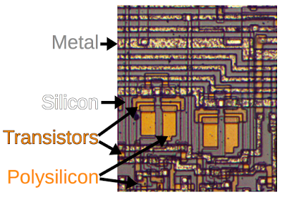
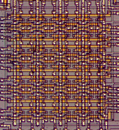
What layers does our crystal consist of? To answer this question we will make the increase even stronger. Now we see 3 layers: the topmost one is metallic electrically conductive. Below it is a layer of polycrystalline silicon, under a microscope it has an orange color. Even deeper - a silicon gray substrate with filler particles forming a semiconductor. The substrate is difficult to see, but you can see black lines between pure silicon and silicon with additives.

Now let's see how the power bus chip (blue and red lines) and the data bus (rainbow line) were located on the chip. The data bus connects the ALU on the right with the command register, the storage register and the address stack on the right. Power distribution was also a daunting task. In the first microprocessors there was only one metal layer, and it had to be arranged in such a way that there were no shorting intersections.
And this is what the processor register 8008 looks like. It consists of an array of 8x7 DRAM cells, each of which uses 3 transistors to store one bit. Each row is one of the seven 8-bit registers (A, B, C, D, E, H, L). On the left you can see horizontal lines for reading and writing, on top vertical lines for reading and writing bits and power lines. Using DRAM in registers instead of static triggers is also unusual. This is probably due to the fact that Intel, initially engaged in memory, had more experience with DRAM.
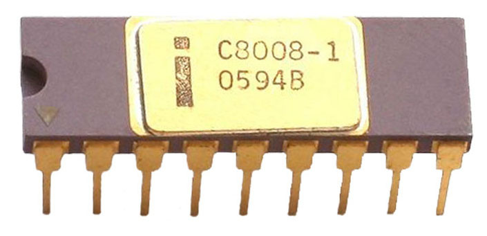
Perhaps, something in the Intel 8008 device will seem to you primitive, if not completely doubtful. Like all devices in the world, the processor was not without flaws, some of which were already visible then. For example, for inexplicable technical reasons, the 8008 had only 18 legs, and the transfer of the full set of data bits and addresses took as many as 3 I / O cycles. The problem was obvious, and the next processor, the i8080, already had 40 legs. But, on the other hand, do not forget: 45 years have passed. From a human point of view, this is a lot, and by the standards of processors it’s just a galactic-sized distance. From these positions and let's look at this remarkable product.
All Articles