Stop slacking off printed circuit boards at home - order them at work.
 In my last article about Intercom with MQTT, I conducted a survey on which article to write next. The choice fell on the order of production of printed circuit boards, here's a little talk about it. If the article goes, I will write on the following topic from the poll.
I do not in any way force immediately to pour out your ferric chloride / hydrogen peroxide, leave them for prototyping. I just want to show that ordering motherboards at work in our time is not at all difficult, as it may seem to a beginning radio amateur. There is something magical in this - to hold in their hands a beautiful board of their own making.
For me, electronics acts as a hobby, and I, spreading the next board, simply send it to production and return to it only after receiving the finished boards. Thus, I can run several projects at the same time. I do not persecute the board myself, and I only mock on the wires as a last resort.
The article will touch on the minimum preparation for the production of boards in the program Eagle CAD. I do not use other programs, but I think the meaning will be something like this.
Well, let's start with the fact that Eagle CAD (hereinafter I will sometimes call it the Eagle) - the program itself is paid, but there is a free version with limitations. For one project, it is allowed to draw no more than 2 sheets of the scheme and dilute no more than 2 layers of the board with an area of up to 80 cm2. I still have enough. But I always use the current version from the manufacturer’s site, and not some broken junk.
I will not teach to work with the program, for this there are good articles from DiHalt (the link will be at the end of the article), but I will quickly go over what needs to be done to order the boards.
PCB layout and DRC control
Before starting the wiring, it is necessary to familiarize yourself with the standards that the manufacturer permits during manufacture - these are the minimum allowable dimensions and clearances. It depends on them how much you get the correct fee. To start the layout, the main thing among them is the minimum size of the track and vias. Manufacturers always indicate their technological capabilities on the site and almost all now make tracks from 6 mil (0.150 mm). Of course it is possible and less, but more often it will be more expensive. I advise you not to shrink and grow larger - it will be more convenient for you later.
Let's say you somehow lit the PCB. Now you need to check the gaps in automatic mode throughout the board. Manufacturers sometimes attach files to control them in different programs. Here, for example, OSH Park has prepared its standards in the files for download . In principle, according to these standards, it is also possible to order from other manufacturers, everywhere the technological capabilities are approximately the same.

* Open the downloaded file in the DRC point or adjust the gaps yourself.
Click Check and get a bunch of errors. For each error, you can look at the place where it is caused, and make a decision: either to correct, or to score and do nothing. Ordering the boards is a simple procedure: what you draw is what you get, the task of the program is just to tell you the weak points.

Upload to manufacturer’s website
All manufacturers accept fees in the form of gerber files, but there are pleasant exceptions. For example, the same OSH Park allows you to download directly * .brd file from Orel or * .kicad_pcb from KiCAD program, followed by viewing the resulting result.
Cam processor
Let's go back to the gerber files. To generate these files from the Eagle, a so-called CAM processor is needed. This is a file in which layers are configured in which file to output.
Of course, you can customize the output yourself from the manufacturer’s website for the same requirements, or you can use it ready if you find it.
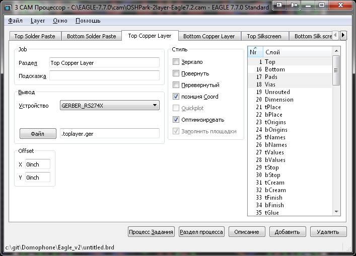
* Eagle will display the top, pads, vias layers in the * .toplayer.ger file
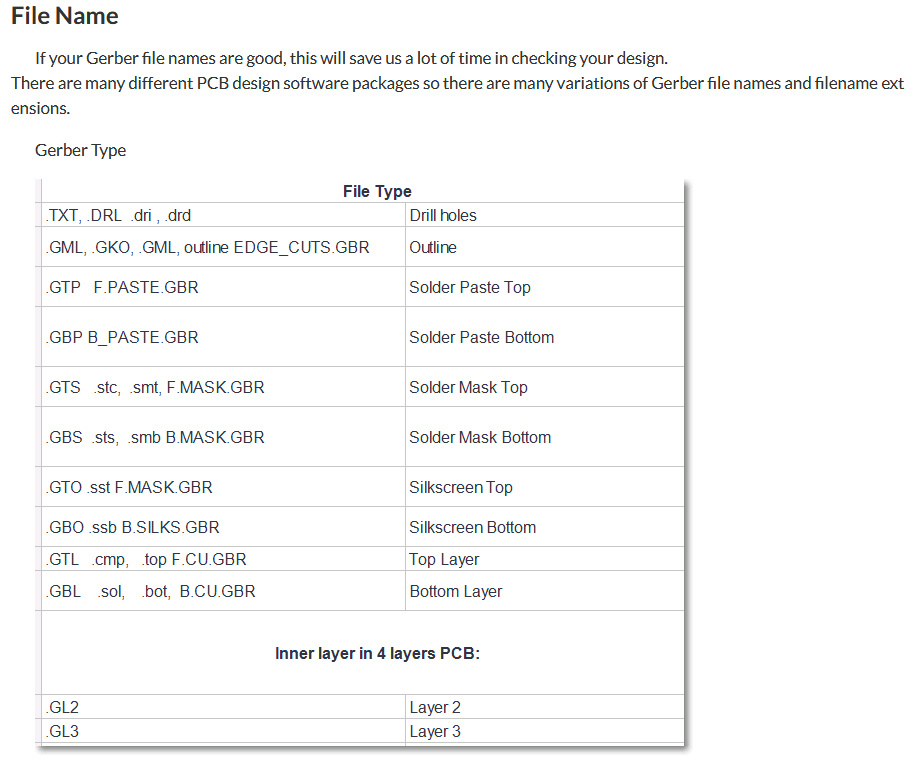
But here you have to be careful, because this CAM processor will output files with names that will be understandable to one manufacturer, and the other will get confused in them. So we look at the requirements for the names of the gerber files on the manufacturer’s website and name them accordingly.
* requirements from the site of one of the manufacturers
Preview gerber files
Before you pay the order will not be overly look at how your files are generated.
Perhaps there was a layer of silk-screen printing or dropping fonts (the most common problems, always write with vector fonts).
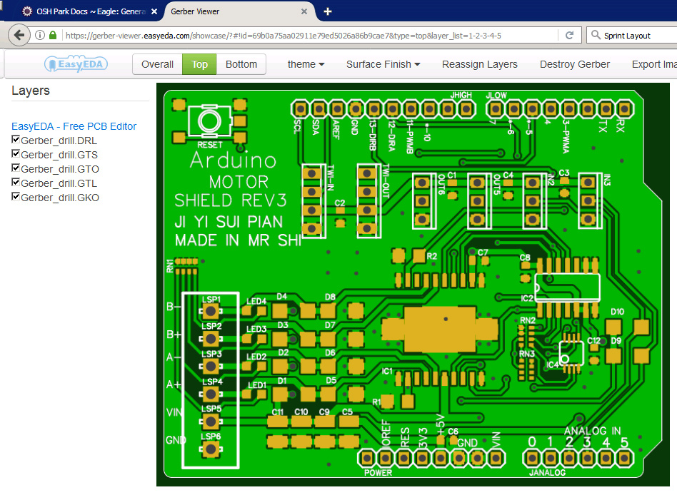
To do this, there are various free online services or programs. Files are downloaded in a zip archive . Sometimes the view function is built right into the board's order form. For example, EaseEDA has its own viewer.
Well, how to pay for the order, I already think you will understand. Thank you for attention.
References:
1. Work in Eagle Cad - a series of articles from DiHalt'a
2. Down with Sprint Layout, long live Eagle Cad - and here I once wrote about working with the Eagle
3. Proven manufacturers of printed circuit boards (always compare prices): OSH Park , EasyEDA , iTead , Seeed Studio
4. Online browsers of gerber files: EasyEDA , Gerber-Viewer
All Articles